
Enhanced thermoelectric properties in two-dimensional monolayer Si2BN by adsorbing halogen atoms?
2021-03-19 03:21ChengWeiWu吳成偉ChangqingXiang向長青HengyuYang楊恒玉WuXingZhou周五星GuofengXie謝國鋒BaoliOu歐寶立andDanWu伍丹
Chinese Physics B 2021年3期
Cheng-Wei Wu(吳成偉), Changqing Xiang(向長青), Hengyu Yang(楊恒玉), Wu-Xing Zhou(周五星),?,Guofeng Xie(謝國鋒), Baoli Ou(歐寶立), and Dan Wu(伍丹)
1School of Materials Science and Engineering&Hunan Provincial Key Laboratory of Advanced Materials for New Energy Storage and Conversion,Hunan University of Science and Technology,Xiangtan 411201,China
2College of Information Science and Engineering,Jishou University,Jishou 416000,China
3School of Physics and Electronic Science,Changsha University of Science and Technology,Changsha 410114,China
Keywords: density functional theory,thermoelectric effects,transport properties,electronic structure
1. Introduction
Thermoelectric(TE)materials can directly convert waste heat into electricity and vice versa, which provide an effective way for the solution of the global energy crisis without producing new contaminants.[1-3]TE materials have attracted intense research efforts due to the huge demand for energy harvesting and power generation. The TE efficiency of the material is measured by the dimensionless figure of merit,ZT =Sσ2T/(κe+κp), where T is the temperature, S is the Seebeck coefficient,σ is the electrical conductivity,κeis the electronic thermal conductivity,and κpis the phonon thermal conductivity.[4-7]
According to the formula, high Seebeck coefficient S,high electrical conductivity σ, low phonon thermal conductivity κpcan obtain high ZT.[8]However, these physical parameters S, σ, and κeare dependent on each other, e.g., the Wiedemann-Franz law indicates σ ∝κe, which causes the TE efficiency to be relatively low. Although the theoretical studies have showed that low-dimensional nanoscale systems can contribute to boosting the TE performance originated from the enhancement of phonon scattering and quantum confinement effect, the ZT of most perfect structures is still low because of their high thermal conductivity, such as graphene(2876 W/m·K),[9]borophene(κzig=72 W/m·K,κarm= 145 W/m·K),[10]MoS2(κzig= 54 W/m·K, κarm=33 W/m·K),[11]etc. Therefore, it is necessary to find appropriate means to reduce phonon transport to improve the TE performance. What is more, the TE parameter κpis the relatively independent quantity that can be changed by some method.[12-18]
In recent years,the thermal transport of low-dimensional nanomaterials has become a research hotspot. Theoretically,by manipulating the phonons or elastic waves that propagate and scatter, the beneficial thermal transport properties can be obtained. Research shows that surface functionalization is one of the feasible and effective manipulation methods.[19,20]This method has been used to regulate the thermal transfer of nanostructured materials composed of group-IV and group-V nonmetallic elements. For example, Wang et al.[21]reduced the thermal conductivity of graphene by depositing gold nanoparticles on its surface by physical deposition. The decrease of the thermal conductivity is mainly attributed to the suppression of ZA phonon modes. Liu et al.[22]improved the thermal conductivity of silene system by full hydrogenation.Although full hydrogenation increases the buckling degree of the silene system, the elimination of asymmetric π-bond is considered to be the main reason for the decrease of phonon scattering rate and the increase of thermal conductivity of hydrogenated silene. Sun et al.[23]studied the effect of oxygencontaining functional groups on the thermal conductivity of reduced graphene oxide by molecular dynamics simulation.Overall, these results are all attributable to the effect of sp3hybridization introduced by surface functionalization on the material.
Moreover, surface functionalization not only can change the heat transport, but also can change the electron transport properties. For example,Xu et al.[24]reported that monolayer C4N functionalization with adsorbing Li, Na, Be, Mg, Ti, V,Cr,and Mn atoms,resulting in the transformation of C4N from semi-metal to semiconductor. By the first principles calculation, Nguyen et al.[25]found that the bandgap can be opened when the concentration of halogen atoms adsorbed on both sides of silicon is greater than 0.25. Therefore, surface functionalization is an effective way to improve the performance of two-dimensional(2D)materials in a specific field. Particularly, halogen atoms have strong electronegativity, which can bind free electrons on the surface of 2D materials and play a role of surface passivation.In order to open the bandgap of 2D materials with metal or semi-metallic properties,halogen is a good adsorption candidate.[26]
Si2BN,which was reported by Andriotis et al. in 2016,is also a kind of graphene-like monolayer structure.[27]It has attracted the interest of researchers in hydrogen storage,battery,and other fields,[28-31]but there have been no reports of any research on TE properties. Because the crystalline structure of Si2BN is more complex than graphene, we predict that it has lower phonon thermal conductivity,which is beneficial to the improvement of TE properties. Nevertheless, the electronic energy band of Si2BN shows its routing metal property, this is negative for TE properties. In theory, by adsorbing halogen atoms on Si2BN,the hybrid type changes from sp2to sp3,resulting in bandgap opening.[32]Moreover,it also breaks the plane structure of Si2BN, the lattice thermal conductivity is further reduced by increasing phonon scattering.
In this work, we research the thermoelectric transport properties of Si2BN adsorbing halogen atoms (Si2BN-4X,X = F, Cl, Br, and I) by using the first principles calculation and Boltzmann transport theory. By adsorbing halogen atoms, the band gap of Si2BN is opened, which leads to the increase of the Seebeck coefficient. In particular, Si2BN-4I has the largest Seebeck coefficient because of the band degeneracy. In addition, the absorption of halogen atoms increases the phonon scattering,and the lattice thermal conductivity decreases significantly, which leads to a significant increase in the thermoelectric properties.
2. Methodology
First-principles calculations are performed based on density functional theory (DFT) using the Vienna ab-initio simulation package (VASP).[33,34]We choose the generalized gradient approximation (GGA) in the Perdew-Burke-Ernzerhof(PBE)parametrization for the exchange-correlation functional.[35]The crystal structure is relaxed with total energy convergence criterion of 10?6eV,the force convergence criterion is 10?4eV/?A, and adopts plane-wave basis with kinetic energy cutoff of 500 eV. The 11×11×1 Γ-center k-mesh is used, and the normal vacuum distance is large than 15 ?A to prevent any physical interactions between the consecutive layers. VASP is used to obtain the second-order interatomic force constant by the finite displacement method with 3×3×1 supercell and 1×1×1 k-mesh, and then the dynamic matrix is constructed by the Phonopy program,and the dynamic matrix is diagonalized to obtain the phonon spectrum.[36]
Based on Boltzmann transport theory, we use VASP combined with BoltzTraP program to calculate the electronic transport properties of materials.[37]The TE transport parameters are calculated using the relaxation time approximation method, where the relaxation time constant τ is 10?14s.This constant has been widely used in the calculation of electron transport properties and reliable results have been obtained.[38,39]Moreover,the TE transport coefficient is converged by using the k-mesh of 20×20×1 in the Brillouin zone(BZ).[40,41]
We calculate the phonon thermal conductivity based on linearized phonon Boltzmann transport equation (PBTE)within relaxation time approximation.[42,43,45]Along the specified direction, the thermal conductivity of monolayer Si2BN and its halide in each branch λ can be described as

where S is the area of the sample,vλis the phonon group velocity of λ branch along the specified direction,which is equal to dω/dq, ω is the phonon frequency for branch λ at wave vector q, τλis the phonon relaxation time of λ branch, and cphis the volumetric specific heat of each mode,which can be calculated with the following formula:


where γλ, M, ωD,λare the Gr¨uneisen parameter, the mass of unit cell, and the Debye frequency of branch λ, respectively.V is the unit cell volume and V0is the completely relaxed unit cell volume. dωλ(V)/dV is the first derivative of the phonon frequency of branch λ with the volume.[49]
3. Results and discussion
Two optimized structures, named Si2BN and Si2BN-4X,are shown in Figs. 1(a) and 1(b), respectively. In top view of Fig.1(a), the lattice constants of Si2BN are a=6.35 ?A,b=6.45 ?A and the bond length between atoms are lSi-Si=2.24 ?A, lSi-N=1.76 ?A, lSi-B=1.95 ?A, and lB-N=1.46 ?A,which are in good agreement with the previously reported ones.[50]In side view of Fig.1(a), the Si2BN shows a plane structure, while the Si2BN-4X (X =F, Cl, Br, I) shows the buckling structure when the surface of Si2BN adsorbs halogen elements, as shown in the side view of Fig.1(b), which is due to the change of the hybrid type of Si-Si atoms. The previous work pointed out that the buckling structure is more beneficial to increase phonon scattering and decrease phonon thermal conductivity.[51]

Fig.1. Top and side views of the geometric structure of (a) Si2BN and(b)Si2BN-4X (X =F,Cl,Br,I).
In Fig.2(a), the electronic band structure of Si2BN presents a metal characteristic and the result matches that of Singh et al.[29]well. However, the materials with insulator or metal property are not good TE materials even though they have a large conductivity or Seebeck coefficient than semiconductor materials.
Therefore, a suitable method to open the bandgap for Si2BN should be applied. When the halogen atoms are adsorbed on the four Si atoms of surface of Si2BN (named Si2BN-4X, X =F, Cl, Br, I), as shown in Fig.3, the electronic structure property of Si2BN transforms from metal to indirect bandgap semiconductor. In addition,the bandgap increases from 1.32 eV of Si2BN-4F to 1.88 eV of Si2BN-4I with the increase of atomic mass of adsorbed halogen, which is presented in Figs. 3(a)-3(d). It is worth mentioning that the electron band structure shows that Si2BN-4X has flat conduction band minimum (CBM) and valence band maximum(VBM),indicating that it has high effective carrier mass, low carrier mobility, and low conductivity, which leads to high S eventually.[52]In addition, the degeneracy of the electronic band structure of Si2BN-4I at the M point in BZ means a large S,which is beneficial to the improvement of ZT.[53-55]

Fig.2. (a)The electronic band structure and(b)DOS of Si2BN.

Fig.3. The electronic band structure of (a) Si2BN-4F, (b) Si2BN-4Cl,(c)Si2BN-4Br,(d)Si2BN-4I.
In order to prove the dynamic stability of Si2BN and Si2BN-4X, we use the finite displacement method to calculate the phonon spectrum. In Fig.4,the results show that there are no imaginary frequencies in the whole BZ,indicating the dynamical stability of Si2BN and Si2BN-4X. In the phonon spectrums of Si2BN and Si2BN-4X,there are multiple phonon gaps in the frequency range from 15 THz to 40 THz. Besides,there are typical strong hybrid features between low-frequency optical branches and acoustic branches in Si2BN and Si2BN-4X. These characteristics indicate that the phonon thermal conductivity of Si2BN and Si2BN-4X will be relatively low.Importantly, as shown in Figs. 4(b)-4(e), there are more and more low-frequency flat optical branches from the Si2BN-4F to Si2BN-4I structure, which means that the phonon thermal conductivity will decrease with the increase of atomic mass of the absorbed halogen.[56]

Fig.4. The phonon dispersion spectra of (a) Si2BN, (b) Si2BN-4F,(c)Si2BN-4Cl,(d)Si2BN-4Br,(e)Si2BN-4I.
On the other hand, in order to prove the thermodynamic stability of halogen atoms adsorbed Si2BN, we calculate the adsorption formation energy of halogen atoms on Si2BN surface as shown in Table 1. According to the definition of adsorption formation energy, the formula for our system can be written as
where Eb[Si2BN-4X], Eb[Si2BN], Eb[X2] are the bind energy per atom of Si2BN-4X, the bind energy per atom of Si2BN,and the bind energy per atom of X2,respectively. n is the total number of Si2BN-4X,nXis the number of adsorbing halogen atoms. Efis the adsorption formation energy per adsorbing halogen atom of Si2BN-4X.
The unit adsorption formation energies of the X atom on the Si2BN are all above 1 eV/atom as shown in Table 1. This means that the binding energy of Si2BN-4X is larger,and the energy released by the formation of Si2BN-4X from isolated atoms is greater than that of Si2BN and X2. Therefore, the lower total free energy of Si2BN-4X demonstrates that the adsorption of X2by Si2BN is experimentally feasible.

Table 1. The adsorption formation energy of halogen atoms adsorbed by Si2BN is calculated. Ef[Si2BN-4X] is the adsorption formation energy per adsorbing halogen of Si2BN-4X,Eb[Si2BN-4X]is the bind energy per atom of Si2BN and Si2BN-4X,and Eb[X2]is the bind energy per atom of X2.
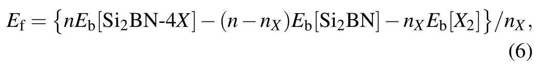
The Si2BN and Si2BN-4X have 2D hexagonal structures.We can study the TE properties along the armchair and zigzag directions. Firstly,we focus on the armchair direction. In order to systematically study the TE properties of Si2BN and Si2BN-4X along the armchair direction at room temperature,we calculate the Seebeck coefficient S, electrical conductivity σ, electronic thermal conductivity κe, power factor PF,phonon thermal conductivity κp, and ZT based on the average temperature T of 300 K and electron constant relaxation time τ of 10?14s. All the results are plotted in Fig.5. As shown in Figs.5(a)-5(b),the S of Si2BN-4X is larger than that of Si2BN;moreover,S decreases and σ increases with the increase of charge carrier concentration n, which is due to the Pisarenko relation.[57]However,the PF of Si2BN and Si2BN-4X appear a maximum as n increases,and the maximal PF of the former is much lower than that of the latter,indicating that the optimal TE performance of Si2BN-4X can be realized at some carrier concentration.
As can be seen from Fig.5(d),the electronic thermal conductivity displays similar behavior to the conductivity. In addition, we can see that the phonon thermal conductivity of Si2BN-4X is lower than that of Si2BN in the temperature range from 200 K to 800 K,as illustrated in Fig.5(e).It is worth noting that the phonon thermal conductivity κpof Si2BN-4I is the lowest among all structures. According to the TE formula,we calculate the TE figure of merit as a function of carrier concentration, as shown in Fig.5(f). The ZT values of Si2BN-4X are significantly greater than that of Si2BN, regardless of the change in carrier concentration. Meanwhile,the ZT curve of Si2BN-4X increases firstly and then decreases with the increases of carrier concentration,where the ZT value of Si2BN-4I is the largest compared to others structures. At 300 K,the ZT maximum of Si2BN is only 0.03, while that of Si2BN-4I reaches 0.50,which is about 16 times that of Si2BN.
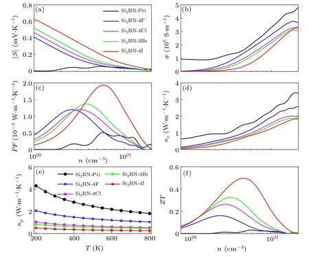
Fig.5. (a) The Seebeck coefficient, (b) electrical conductivity, (c) power factor, (d) electronic thermal conductivity, (e) phonon thermal conductivity,and(f)ZT of Si2BN and Si2BN-4X along armchair direction.
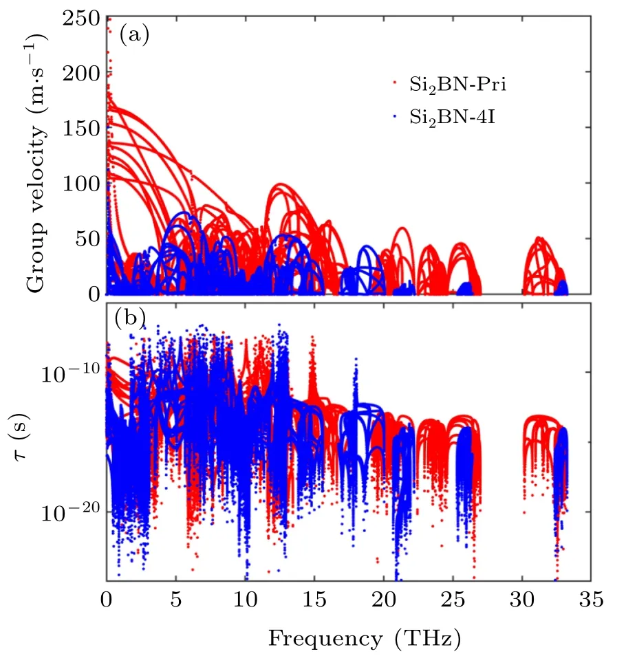
Fig.6. (a) The group velocity and (b) phonon lifetime of Si2BN-4I along armchair direction.
From the above results, Si2BN-4I is the optimal structure for TE performance,which stems from the lowest thermal conductively after the surface functionalization. The phonon thermal conductivity of Si2BN-4I is only 0.41 W/m·K while that of Si2BN is 3.38 W/m·K at 300 K.In order to explain the decrease of phonon thermal conductivity of Si2BN-4I compared with that of Si2BN in armchair direction, we calculate the group velocity and phonon lifetime along the armchair direction.Figure 6(b)shows that the Si2BN-4I has multiple wide optical-optical gaps in the range from 15 THz to 35 THz.Therefore, the decrease of phonon thermal conductivity of Si2BN-4I compared with Si2BN results from the decrease of the group velocity.[53]
In order to study the effect of temperature on thermoelectric properties, the TE performance of the armchair direction of Si2BN-4I at the temperatures of 300 K,500 K,and 800 K is calculated and shown in Fig.7. As the temperature increases,the PF of Si2BN-4I increases(in Fig.7(c)),while the phonon thermal conductivity of Si2BN-4I decreases(in Fig.7(e)). As a result,the ZT value of Si2BN-4I increases with the increase of temperature(in Fig.7(f)),and the ZT of Si2BN-4I can reach 0.8 at 800 K.However,compared with Figs.7(c)and 7(f),the optimal ZT carrier concentration (NZT) has a large deviation from the optimal PF carrier concentration (NPF), and the PF corresponding to NZTis relatively low. Obviously,with the increase of temperature,NPFbecomes lower,S corresponding to NPFdecreases very slight, and the increase of electrical conductivity σ is also very small.But with the increase of temperature,the increase of κecorresponding to NPFis much greater than that of κp, and the value of κeis an order of magnitude higher than that of κp. Therefore, κeplays a major role that influences the ZT with the change of temperature, and NZTmoves towards the lower κe. This limits the improvement of ZT to some extent, and the excessive κealso indicates that there is still space for improvement of the TE performance of Si2BN-4I.[58]

Fig.7. (a) The Seebeck coefficient, (b) electrical conductivity, (c) power factor, (d) electronic thermal conductivity, (e) phonon thermal conductivity,and(f)ZT of Si2BN-4I along armchair direction at 300 K,500 K,and 800 K,respectively.
Fig.8. The ZT of Si2BN and Si2BN-4X along zigzag direction at 300 K.
The above calculations of TE properties are based on the armchair direction. In Fig.8(a), we obtain the ZT values of Si2BN and Si2BN-4X at 300 K along the zigzag direction. In the zigzag direction of Si2BN-4I, we draw the same conclusion as in the armchair direction, but the TE performance in the zigzag direction is slightly lower than that in the armchair direction, so we mainly introduce the TE performance in the armchair direction. The similar conclusions can be obtained in the zigzag direction.
4. Conclusion
In this work, we study the electron transport, thermal transport, and thermoelectric properties of Si2BN adsorbing halogen atoms(Si2BN-4X,X=F,Cl,Br,and I)using the first principles calculation and Boltzmann transport theory. The adsorption of halogen atoms can significantly regulate the energy band structure and lattice thermal conductivity of Si2BN.The band gap of Si2BN is opened by adsorbing halogen atoms,which leads to the increase of Seebeck coefficient. In particular, Si2BN-4I has the largest Seebeck coefficient because of the band degeneracy. In addition, the absorption of halogen atoms increases the phonon scattering,and the lattice thermal conductivity decreases significantly, which leads to a significant increase of ZT.
猜你喜歡
今日中國·西班牙文版(2022年11期)2022-11-05
中國自行車(2022年6期)2022-10-29
湘潮(上半月)(2019年9期)2019-05-22
知識經濟·中國直銷(2018年6期)2018-06-29
知識經濟·中國直銷(2017年7期)2017-07-24
世界汽車(2017年6期)2017-06-19
讀寫算(上)(2016年3期)2016-11-07
知識經濟·中國直銷(2016年12期)2016-02-27
世界汽車(2014年7期)2014-08-06

- Chinese Physics B的其它文章
- Transport property of inhomogeneous strained graphene?
- Beam steering characteristics in high-power quantum-cascade lasers emitting at ~4.6μm?
- Multi-scale molecular dynamics simulations and applications on mechanosensitive proteins of integrins?
- Enhanced spin-orbit torque efficiency in Pt100?xNix alloy based magnetic bilayer?
- Soliton interactions and asymptotic state analysis in a discrete nonlocal nonlinear self-dual network equation of reverse-space type?
- Discontinuous event-trigger scheme for global stabilization of state-dependent switching neural networks with communication delay?