
Weakening effect of plastic yielding inception in thin hard coating systems?
2021-03-19 03:21XiaoHuang黃嘯ShujunZhou周述軍andTianminShao邵天敏
Chinese Physics B 2021年3期
Xiao Huang(黃嘯), Shujun Zhou(周述軍), and Tianmin Shao(邵天敏)
1School of Mechanical Electronic and Information Engineering,China University of Mining and Technology,Beijing 100083,China
2State Key Laboratory of Tribology,Tsinghua University,Beijing 100084,China
Keywords: plastic yielding,weakening effect,spherical nanoindentation,PVD coating
1. Introduction
Hard coatings can effectively improve surface tribological performance, especially in reducing friction and promoting resistance to corrosion and wear.[1,2]Classical wear theory emphasizes surface hardness as the key factor of wear resistance. In the last decades,physical and chemical vapor deposition(PVD and CVD)enabled the fabrication of various hard and even super-hard coatings.[3,4]However, the failure origination of a coating/substrate system in friction and wear is complicated,not only abrasive wear on the top surface but also coating fracture in the subsurface and plastic deformation in the substrate can cause the coating failure.[5-8]Particularly for the PVD and CVD coatings whose thickness ranges from hundreds of nanometers to a few microns,substrate plastic yielding could be the premature failure in a coating/substrate system. The plastic flow of substrate material permits the flexure of coating and induces additional tensile stress in the coating,accelerating the initiation and propagation of cracks within the coating material.[9,10]Therefore, it is significant to promote the plasticity onset threshold of the substrate for enhancing the tribological performance of a coating/substrate system.
The behavior of substrate yielding relates more closely to the coating thickness and substrate properties rather than the coating hardness.[8]Several publications revealed that thin hard coating on soft substrate does not necessarily result in better tribological performance. Conversely, it may cause weakening effect of the resistance to plastic yielding in the substrate due to additional stress. Komvopoulos found that indentation of thin hard coatings on soft substrates may cause higher substrate stresses compared with a non-coated case using the finite element method (FEM).[11]It is worth noting that the hard coating is defined as the coating’s elastic modulus and hardness is relatively higher than the substrate. Therefore the weakening effect could extensively exist in any hard coating/substrate systems when the coating thickness is not appropriately designed regardless of the coating deposition techniques. In a following paper, Komvopoulos pointed out such higher stresses have a weakening effect on the threshold to plastic yielding of the coating/substrate system.[12]Sun studied the contact mechanics between a rigid sphere and compliant substrates coated with TiN coating using the FEM.[13]The paper found that the critical load of yielding inception in the coated system is smaller than that of the uncoated substrate, demonstrating that the hard coating weakens the substrate’s load carrying capacity. Recently,Goltsberg et al.[14,15]studied the plasticity onset in a coated sphere loaded by rigid flat using the FEM. The results showed that the weakening effect is closely related to the elastic modulus mismatch between coating and substrate. Song et al.[16]studied the plasticity onset in a coated flat contact with a rigid sphere by the FEM and showed similar result with Ref. [14]. In addition to these theoretical studies, there are also a few experimental investigations of weakening effect. Our previous studies[17,18]qualitatively validated the weakening effect model in Ref.[14]using elastic-plastic index (EPL) and showed experimentally that thin hard coatings can reduce the coated system’s resistance to plastic yield inception. Afterwards our studies tested the wear properties of TiN and TiAlN coating on different substrates.[19]The results showed that larger modulus and hardness mismatch between coating and substrate could cause the detrimental effect of wear properties. Rebholz et al.[20]tested the pin-on-disk wear rate of Ti-Al-B-N coatings on soft stainless steel substrate(H=5 GPa). The experiments indicated that the relatively hard coating with large Young’s modulus demonstrated a higher wear rate than the coating with moderate hardness and modulus. As can be seen from the above-mentioned literature,the weakening effect has been theoretically proposed several times by the FEM. However,the FEM has the limitation on the element mesh density,so it could be difficult to simulate the model with the coating thickness in the range of micron and submicron. Meanwhile, the detailed study on the origin and influencing factors of weakening effect is still missing. In this study,by utilizing the image charges method in contact mechanics,[21]the stress distribution in a coated system is evaluated analytically to interpreter the origin and influencing factors of weakening effect.Moreover, the experimental validation of weakening effect is indeterminate. In the preview studies,the authors proved that potential weakening effect existed in coated system using indirect methods.[17,18]In this study, the spherical nanoindentation tests are applied to convert the load-displacement curve into a more meaningful stress-strain curve to identify the yielding point.[22,23]The yielding threshold of coated and uncoated single crystalline silicon are compared directly to validate the credibility of weakening effect. This paper is organized as follows: Section 2 presents the theoretical background of stress simulation and spherical nanoindentation. Section 3 describes the experimental methods,Section 4 give the results of simulation and experiments,and finally the conclusion is provided.
2. Theoretical background
2.1. Plastic yielding in spherical contact
Figures 1(a) and 1(b) schematically show a rigid sphere(radius=R)in contact with an uncoated elastoplastic flat and a coated elastoplastic flat, respectively. The classical Hertz theory provides the following relations between contact load P and interference hein the case of a homogenous flat elastically deformed by a rigid sphere:

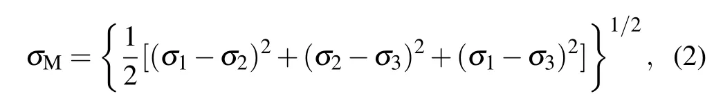
where E and ν are the elastic modulus and Poisson’ ratio of the flat. The von Mises yielding criterion can be used to determine the elastic-to-plastic transition point in this study as the following expression:
where σMis the von Mises stress,σ1,σ2,and σ3are the principal stresses. When σMexceeds the yielding strength Y of the flat material, the plastic yielding occurs. Combined the Hertz theory and von Mises criterion, the critical load that initiates the plastic yielding in a homogenous flat can be expressed as[15]

where Cvis the function of Poisson’s ratio in the form of Cν=1.234+1.256ν.

Fig.1. Schematic of spherical contact. (a)uncoated surface(b)coated surface.
However,when the homogenous flat is coated,the Hertz theory is no more valid to evaluate the stress distribution. In this study,the stress distribution and plastic yielding inception in the coated flat is solved by commercial FilmDoctor software. The software is based on the image charges method,which is well-known in electrodynamics. The image charges method is completely analytical which can be expressed in elementary functions and closed form.[21,24]In contact mechanics,the method treats all the surfaces and interfaces as boundaries where special stress and strain conditions should be satisfied. In this study,the interface between coating and substrate is assumed to be well-bonded,therefore,the displacement,the stress normal to the interface and the shear stress are identical at both sides of the interface. The stress parallel to the interface and the strains are different at two sides of the interface. Based on the above boundary conditions, the principal stresses along the depth are evaluated and simultaneously used to calculate the von Mises stress to determine the yielding point. The load-displacement relation solved by FilmDoctor was compared with the Hertz theory to verify the accuracy of the software. The difference between two methods is less than 0.5% which is more accurate than the FEM with the error of 2.5%.
2.2. Nanoindentation stress-strain curve
Figure 2 schematically shows the geometry of a spherical nanoindentation test. The total interference htconsists of elastic portion heand plastic portion hp. The widely used Oliver and Pharr method utilizes the unloading slope to determine the heby differentiating Eq. (1) with respect to h and yields the following expression:

Substitute Eq.(4)to Eq.(1)to result the following expression:

where dP/dh is the stiffness S of the unloading part of the indentation load-displacement curve, which can be determined from the unloading slope. Therefore, the hecan be evaluated by the following expression:

Once heis determined,the contact depth hccan be calculated.The contact depth hcis defined as the distance from the contact point to the maximum interference. Sneddon[25]showed that the elastic interferences above and below the contact point are equal to each other. Therefore, hccould be given in the following expression:[26]

Afterwards,the contact radius a can be given by

Note that heequals htwithin the elastic limit, so the indentation radius a can be simplified to a2=he·R when the deformation is purely elastic. Combining Eqs.(1)and(8)yields


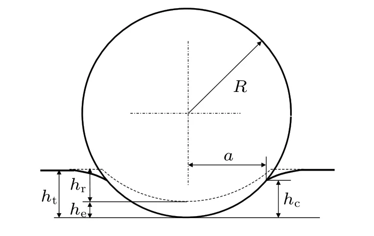
Fig.2. Schematic of spherical nanoindentation.
The above theory is based on the spherical indentation test on a homogenous flat. When the flat is covered with coating, the linear relationship between σ and ε is still valid,but the ratio between σ and ε is determined by the effective modulus which is the function of the moduli of both coating and substrate and coating thickness.
3. Experimental details
3.1. Specimen preparation
The (100)-oriented single-crystalline silicon wafer and polished copper were used as substrates for coating deposition. Tungsten (W) coatings were deposited on silicon and copper substrates by an ion beam assisted deposition(IBAD)system.[27]with the thickness of 700 nm and 600 nm respectively. In the IBAD system, the assisted ion beam could impact the coating atoms onto the substrate to improve the binding force between coating and substrate. For the deposition process, the vacuum chamber was first exhausted to a base vacuum pressure of 3.5×10?4Pa to remove impurity gases.Following this,working gas Ar was introduced into the chamber and pressurized to 1.0×10?2Pa to start the ion arc. The substrates were bombarded by the assist ion source for 10 min for decontamination prior to the coating process. During the deposition process,the working current of the ion sources was 80 mA with energy of 2500 eV. In order to obtain uncoated specimens for comparison,several silicon and copper samples were masked with tin foil and placed adjacent to the samples to be coated. This was carried out to avoid possible heat induced differences between the coated and uncoated samples.
3.2. Properties of measurement
The nanohardness and elastic modulus of the tungsten coating, the silicon substrate and the copper substrate were measured by the nanoindentation system (CSM Instrument Nanoindentation Tester NHT2)using pyramidal Berkovich tip with a force of 2 mN.For the nanohardness and elastic modulus tests, 20 repetitions were carried out in a 4×5 matrix and 20 μm apart. Poisson’s ratio of the silicon, copper and tungsten coating is assumed to be 0.3 in the modulus measurements. The surface roughness is measured using an interferometer(ZYGO NewView 8200).
3.3. Spherical nanoindentation
Spherical indentation tests were utilized to derive stressstrain relations from common load-displacement curves as discussed in Section 2.3. The tests were also carried out on the CSM NHT2 nanoindentation system using a spherical diamond tip with the radius of 20 μm. The partial unloading mode was applied[28]in the test, during which the maximum load was not applied in a single loading segment. Instead,repeated loading-unloading loops were performed with gradually increasing load to accomplish the entire loading process as shown in Figs.3(a)and 3(b). The unloading stiffness S can be derived from each loading-unloading loop and is further used to determine the stress and strain at each load value. The maximum load on the coated/uncoated silicon is 450 mN with 100 loading-unloading cycles and 25 mN on the coated/uncoated copper with 15 cycles since the copper has a much lower elastic limit than the silicon. Five indentation repetitions were carried out to obtain the average results. After indentation tests,a scanning electron microscope (SEM, TESCAN LYRA3) and a focused ion beam(FIB,TESCAN LYRA3)were used to observe the top surface and cross-section of the indention dots to confirm if there is any fracture or delamination in the coating or substrate or at the coating/substrate interface.

Fig.3. Load evolution in partial unloading nanoindentation test: (a)maximum 450 mN on silicon,(b)maximum 25 mN on copper.
4. Results and discussion
4.1. Origin of weakening effect
The von Mises stress criterion was adopted in the plastic yielding judgement in both uncoated and coated substrates.FilmDoctor was used to calculate the maximum von Mises stress inside the substrate material. In order to verify if Film-Doctor’s calculation is accurate,the simulation results is compared with classic Hertz solution and published finite element method (FEM) simulation results,[15]which also focused on the weakening effect. The comparison comes out that Film-Doctor’s analytical simulation has good fits with the Hertz solution and the published FEM results. Thus the simulation results by FilmDoctor should be reliable. Table 1 gives the typical calculation instance of material properties. In the calculation,the coating thickness is 2μm and the substrate thickness is 100μm to eliminate possible influence from the bottom support. When the von Mises stress exceeds the substrate’s yielding strength, the plastic deformation occurs and the corresponding load is marked as the critical load Pc.

Table 1. Input material properties for calculation.

Fig.4. The von Mises stress distribution for(a)the uncoated substrate and(b)the coated system.
The calculated Pcof the uncoated and coated substrate is 17 and 9.5 mN respectively,indicating the presence of weakening effect. Figures 4(a)and 4(b)show the von Mises stress distribution in uncoated and coated cases at the same load P=9.5 mN.Overall,the von Mises stress is continuous in the uncoated substrate. Since the applied load(9.5 mN)is below the yielding critical load (16 mN) of the uncoated substrate,the maximum stress(163.9 MPa)is still within the elastic limit(200 MPa). The maximum stress is located in the subsurface,which is in accordance with the Hertz theory. By contrast,the von Mises stress is discontinuous at the coating/substrate interface in the coated system. The maximum stress(383.9 MPa)is located at the interface inside the coating. Since the PVD coating is much harder than the substrate material, such mild stress cannot initiate plastic yielding in the coating material.However,the von Mises stress in the substrate just reaches the yielding strength(200 MPa)along the interface inside the substrate. Thus the hard coating does not efficiently protect the substrate from plastic yielding and even introduces a weakening effect of loading bearing capacity.
Figure 5 shows the principle stress along the depth at the position of symmetry axis. Notice that along the symmetry axis the shear stresses are all zero(τxy=τxz=τyz=0),so the principle stress equals the corresponding normal stress, i.e.,σz=σ1and σx=σy=σ2=σ3. Under the above conditions,the calculation of von Mises stress can be reduced to the following equation σvon=|σ1?σ2|=|σz?σx|. In the uncoated substrate, σx, σyand σzare continuous and negative, indicating the substrate are in compressive stress state. In contrast,in the coated substrate system,σxand σyare discontinuous at the coating/substrate interface while the σzremains continuous. In the substrate close to the interface, the σxincreases from ?50 MPa without coating to ?30 MPa with coating,while the σzdecreases from ?210 MPa to ?230 MPa. The opposite trend leads to larger gap between σxand σzin the coating/substrate system compared to the uncoated substrate.As discussed above,the calculation of von Mises stress can be simplified to the difference between σxand σz, thus the von Mises magnifies in the coating/substrate system.

Fig.5. Principle stress distribution along the z axis
To further explore the reason of stress growth in the coated system, Figs. 6 and 7 show the normal displacement and strain along the z axis.The normal displacement along the z axis in coated system is continuous at the coating/substrate interface. This is due to the well-bonding between coating and substrate,so the displacement is compatibility at the interface.There is a significant inflection of normal displacement at the interface as shown in Fig.6, so the differential coefficient of displacement, namely the normal strain should be discontinuous at the interface. The result in Fig.7 coincides with the deduction, the normal strain is discontinuous at the interface.According to the generalized Hooke law,the relation between stress and strain is as follows:

Equation (10) can be further converted to the following expression:

According to Eq. (11), with the decrease of εz, the tendency of σxis rising. Indeed, Figs. 5 and 7 demonstrate the εzdecreases and σxincreases in the coated system. Since the principal stress σxis positive, the increasing σxmeans that the principal stress becomes more tensile. Meanwhile,when a hard coating/substrate system is contacted by an indenter,the contact area is smaller than the uncoated substrate and this will cause the principal stress σzmore compressive. This means that the algebraic value of σzdecreases. The opposite change tendency of σxand σzcauses the rise of von Mises stress as shown in Fig.5. It is worth noting that in Eq. (11) σzalso has a function on the value of σx. In the coated system, the decreasing σxcould counteract the decreasing εzand further influences the weakening effect. Thus the influencing factors of weakening effect are complex and will be discussed in detail in Subsection 4.2. Note that weakening effect is caused by the additional stress at the coating/substrate interface under contact force.Different coating technology would not have significant effect on the weakening effect. Whenever the coating’s modulus is higher than the substrate and the coating thickness is inappropriate designed,the weakening effect could exist.

Fig.6. Normal displacement along the z axis.

Fig.7. Normal strain εz along the z axis.
4.2. Influencing factors of weakening effect
The calculation of Pcrequires the dimensional input of specific material properties,such as elastic modulus,yielding strength and coating thickness. In order to acquire the universal dimensionless solution of weakening effect, a wide range of material properties are taken into consideration. The radius R of the spherical diamond tip is set to be 100μm. The coating thickness t varies from 0.1 to 10μm,yielding the dimensionless t/R ratio in the range of 0.001 ≤t/R ≤0.1. The elastic moduli of the coating and substrate vary in the range 300 ≤Eco≤800 GPa and 100 ≤Esu≤600 GPa. The yielding strength of the substrate varies in the range 0.3 ≤Ysu≤1 GPa.The coating material is assumed to be purely elastic in this study to simplify the calculation. Poisson’s ratio of both coating and substrate is set to be 0.3,which has neglected the effect on the calculation results.


Table 2. Mechanical properties of coating/substrate combinations.


In a similar way,(t/R)mwcan be expressed as follows:

Equation (13) shows that (t/R)mwdecreases as Eco/Esubincreases. The (t/R)mwrepresents the dimensionless coating thickness corresponding to the most-weakening effect.Therefore the worst coating thickness becomes smaller when Eco/Esubincreases.

Fig.8. Relation between Pc and(t/R)in different coating/substrate systems: (a)Eco/Esub=2,(b)Eco/Esub=4.
Similarly,the transition thickness(t/R)Tfrom weakening effect to strengthening effect can be expressed in the following equation:

Equation(14)shows that(t/R)Tis determined by both Eco/Esuband Ysub/Esub,yet Ysub/Esubhas a much more signifciant effect than Eco/Esub.
Using Eqs.(12)-(14),the critical coating thickness(t/R)T,the most weakening effect Pc-mwand the corresponding coating thickness(t/R)mwin any given coating/substrate system can be easily calculated to guide the design of a coating system.
4.3. Indentation stress-strain curves
Table 3 shows the mechanical properties and surface roughness of the samples. The W coating is harder and more rigid than silicon and copper substrates. Using FilmDoctor,it is confirmed that 700 nm W coating on silicon and 600 nm W coating on copper both have weakening effect. The silicon,copper and W coating are nanometer scale smooth, which is suitable for performing nanoindentation tests.

Table 3. Properties of the samples.

Fig.9. Nanoindentation stress-strain curves: (a)uncoated silicon,(b)coated silicon,(c)uncoated copper,(d)coated copper.
Using partial unloading nanoindentation test as described in Subsection 3.3, stress-strain test results are illustrated in Figs. 9(a)-9(d). The tests on uncoated silicon wafer have a good repeatability since the wafer surface is nanometer level smooth. The curves in Fig.9(a)does not start from the coordinate origin since a certain stress and strain have been generated at the first indentation point. The red dotted line in Fig.9(a) is obtained by extending the linear relation of the stress-strain curve from the coordinate origin as a reference line. The spherical indentation induced plastic deformation in monocrystalline silicon is not as obvious as that in metal tensile test since the stress field produced by spherical indentation is unique.[29]The maximum von Mises stress beneath spherical indenter is located in the subsurface instead of the top surface. Thus the plastic zone is fully surrounded by the elastic zone,which has a limited influence on the stress-strain curve.With the increasing loading force,the plastic zone gradually expands and stress-strain relationship gradually deviates from the linear relationship. It is worth noting that the plastic deformation in silicon is caused by phase transformation rather than dislocation slip. The crystalline silicon can transfer to amorphous silicon under certain contact stress. Since the amorphous silicon is less rigid than the crystalline silicon and thus exhibits a similar plastic yielding phenomenon in the stress-strain curve. In the uncoated wafer,when the strain value exceeds 0.1 (the corresponding load is about 120 mN),the stress-strain curve shows certain plasticity.In Fig.9(b),the repeatability of tests on coated silicon is slightly lower,which may be caused by the higher surface roughness of the coated sample.There is a linear relationship between stress and strain at the beginning of the curves. When the strain value exceeds 0.08 (the corresponding loading force is about 100 mN), the curves deviate from linear relationship.
Figures 9(c) and 9(d) show the stress-strain curves on coated and uncoated copper. Since copper has a relatively larger roughness and less homogeneity than silicon wafer,the fluctuation in the stress-strain curves on copper is more obvious than silicon. Nevertheless, Figs. 9(c) and 9(d) show that the uncoated and coated copper deviate from linear relationship when the strain exceeds 0.025(the corresponding loading force is about 3.0 mN) and 0.02 (the corresponding loading force is about 2.5 mN),respectively. Therefore the weakening effect is also valid in the coated copper.
For further comparison,Fig.10 illustrates the average results of the above stress-strain tests. In Fig.10(a), when the strain value is less than 0.08,the two curves are basically coincident. When the strain exceeds 0.08, the coated silicon undergoes plastic deformation first, and the uncoated silicon keeps elastic deformation until strain exceeds 0.10. The degree of plastic deformation in the coated silicon is more severe than the uncoated silicon. Therefore the tungsten coated silicon has a weakened threshold of plastic deformation than the uncoated silicon,indicating the existence of weakening effect. In Fig.10(b),the two curves deviate gradually when the strain exceeds 0.01 and the dashed line is above the solid line until strain exceeds 0.05,indicating the coated copper already emerged mild plastic yielding at strain point of 0.01. Meanwhile, the solid line deviates from linear relation when strain exceeds 0.02,indicating that the plastic deformation becomes obvious in the coated copper at the strain point of 0.02. In the uncoated copper,the corresponding point is around strain point of 0.025. The above two phenomena once again indicate that the weakening effect is valid in coated copper. Note that the solid line exceeds the dashed line when the strain is over 0.05. This could be caused by the work hardening under severe plastic deformation which is not the research focus in this study.

Fig.10. Average stress-strain curves: (a)coated and uncoated silicon,(b)coated and uncoated copper.
In Fig.11, SEM and FIB were applied to check the top surface and cross section of the indentation dots to verify if there is any fracture in the coating or debonding at the coating/substrate interface. In the SEM images, the coating and substrate seem to be intact and free from obvious fractures.The coating and substrate is also well bonded without obvious delamination. Thus the fracture and delamination may have negligible effect on the indentation tests. The weakening effect in the stress-strain curves should be caused by the plastic yielding inception in the substrate.

Fig.11. Top surface and cross-section SEM of nanoindentation dots: (a)top surface of W coated silicon, (b) top surface of W coated copper, (c) cross section of W coated silicon,(d)cross section of W coated copper.
5. Conclusions
The stress-strain curves of monocrystalline silicon wafers and polished copper have been obtained using partialunloading spherical nanoindentation tests. The tungsten coated silicon and copper demonstrate a weakening effect of plastic yielding threshold compared with the uncoated samples. This may be the first direct validation of the weakening effect in hard coating systems. The origin of weakening effect is analyzed by stress simulation and the results indicate that the modulus mismatch between coating and substrate could induce extra stress in coating systems and cause the early plastic yielding in coating systems. The dimensionless formula of influencing factors on weakening effect is induced by stress simulation and numerical fitting,which can theoretically guide the optimization design of hard coating systems.

- Chinese Physics B的其它文章
- Transport property of inhomogeneous strained graphene?
- Beam steering characteristics in high-power quantum-cascade lasers emitting at ~4.6μm?
- Multi-scale molecular dynamics simulations and applications on mechanosensitive proteins of integrins?
- Enhanced spin-orbit torque efficiency in Pt100?xNix alloy based magnetic bilayer?
- Soliton interactions and asymptotic state analysis in a discrete nonlocal nonlinear self-dual network equation of reverse-space type?
- Discontinuous event-trigger scheme for global stabilization of state-dependent switching neural networks with communication delay?