
Improved efficiency and stability of perovskite solar cells with molecular ameliorating of ZnO nanorod/perovskite interface and Mg-doping ZnO?
2021-03-19 03:21ZhenyunZhang張振雲LeiXu許磊andJunjieQi齊俊杰
Chinese Physics B 2021年3期
關鍵詞:俊杰
Zhenyun Zhang(張振雲), Lei Xu(許磊), and Junjie Qi(齊俊杰)
School of Materials Science and Engineering,University of Science and Technology Beijing,Beijing 100083,China
Keywords: perovskite solar cells ZnO nanorods, interface modification, preparation parameters, Mg doped ZnO
1. Introduction
The organic-inorganic perovskite light-harvesting materials have the advantages of inexpensive fabrication with solution techniques,strong absorption in the visible spectrum,and high carrier mobility.[1-3]Since the first use of the materials as dye sensitizers in dye-sensitized solar cells with the power conversion efficiency(PCE)of 3.8%,[4]perovskite solar cells(PSCs) have been widely investigated in recent years. The PCE of the PSCs is improving rapidly and now has reached more than 25%.[5-9]
The structure of the PSCs usually includes an anode, a hole transportation layer (HTL), a light absorption layer, an electron transportation layer(ETL),and a cathode.[10-12]The ETL always plays a significant role in transporting electrons and blocking holes. Among different metal oxides applied as ETL,zinc oxide(ZnO)has garnered keen attention due to the superior opto-electronic properties,and they can be regulated by tuning the composition, doping, and morphology.[13-15]In addition, high-quality ZnO can be obtained via solutionprocessed at low temperature.[16]Many attempts have been made in facilitating the PCE of ZnO-based PSCs to over 20%.By tuning ZnO/perovskite interface with sulfidation,the PCE of the ZnO-based device was increased to 20.7%,[17]as well as protonated ethanolamine and MgO.[18]However, the PCE is still lower than the TiO2based PSCs. The difference in PCE may result from the non-optimized ZnO NR crystallinity(conductivity of NR) that impacts the electron transportation between the perovskite absorbing layer and ETL,[19]but may also be owning to the recombination originating from traps at the interface between ETL/perovskite. As a result, it is very important to improve the ZnO NR crystallinity and reduce the trap density at the interface between ETL/perovskite. MgO was applied as a passivation layer to reduce the interfacial traps.[18]Despite the improved efficiency of the device, the preparation process is not simple, and the ZnO-based PSCs are unsatisfactory to be persistent in the air without sealing.Polyvinylpyrrolidone(PVP)is a water-soluble polymer,which was incorporated between ETL and Ag cathode to improve electron transport for inverted PSCs.[20]While whether the PVP interlayer between perovskite and ETL would influence the device performance is interesting.
It is well known that element doping is an effective method to modify the crystallinity and the electrical/optical properties of the material.[21]Magnesium (Mg) is an ideal doping element to regulate the energy band structure of ZnO owing to the similar radius of Mg and Zn. Mg doped ZnO nanocolloidal ETL was applied in PSC, achieving a PCE of 16.5%with low FF.[22]Few studies about Mg doped ZnO NRs in PSC fields were reported.
In this paper,the PVP layer is inserted between ZnO NRs and perovskite material.Steady-state photoluminescence(PL)and x-ray diffraction(XRD)measurements show that the PVP layer helps reduce the interfacial defects and enhance perovskite crystallinity. Meanwhile,it also slows the PSC degradation,and 80%of primary PCE remains after being exposed to air for 30 d without encapsulation. In addition, we incorporate Mg in ZnO NRs and optimize the preparation parameters to improve ZnO NR crystallinity and promote the electron transportation. As a result,photovoltaic parameters of the ZnO NRs based PSCs are enhanced,and a PCE of 19.63%is attained.
2. Experimental details
We used fluorine-doped tin oxide(FTO)transparent glass as the electrode. After etching with zinc powder and hydrochloric acid (HCl) solution, the FTO was cleaned with alkaline detergent, deionized water, acetone, ethyl alcohol,and isopropanol in ultrasonic cleaners. The seed layer was first deposited by the sol-gel method as follows:[23]a solution of Zn(CH3COO)2·2H2O (10 mM) in ethylene glycol monomethyl ether was spin coated at 3000 rpm for 30 s on the FTO substrates, then the FTO substrates with ZnO seed layer were annealed at 350?C for 30 min. The ZnO NRs were prepared by hydrothermal method,[24]zinc nitrate hexahydrate (Zn(NO3)2·6H2O) and hexamethylenetetramine(HMTA) were dissolved in deionized water in equimolar(30 mM). The magnesium nitrate (Mg(NO3)2·6H2O) (0, 1%,2%, 5%, 10%) was added into the precursor solution to induce Mg doping. The FTO substrates with the ZnO seed layer were immersed in the precursor solution and put into the highpressure reaction vessel. The seed layer at 30 mM precursor concentration was kept at 90?C for different growth time(2.5 h,3 h,3.5 h,4 h).Then the FTO substrates with ZnO NRs were rinsed with DI water several times and was annealed at 450?C for 30 min.A PVP solution in deionized water(1 wt%)was spin-coated on the ZnO NRs at 5000 rpm for 60 s and was annealed at 100?C for 10 min.
Perovskite film was prepared by the twostep sequential deposition method[25]ZnO NRs were infiltrated with PbI2by spin-coating a PbI2solution in DMF (1 M) that was kept at 70?C, which adopted a spinning rate of 4000 rpm and a spinning period of 30 s. After keeping on the hot plate at 70?C for 30 min to dry PbI2and cooling to room temperature, the film was dipped into CH3NH3I (MAI) solution in 2-propanol (0.063 M) and then dried for 30 min to form in situ CH3NH3PbI3(MAPbI3) film. The Spiro-OMeTAD solution was prepared by mixing 72.3 mg Spiro-OMeTAD,30 μL 4-tert-butylpyridine and 35 μL bis(trifluoromethane)sulfonamide lithium salt(Li-TFSI)stock solution(260 mg/mL Li-TFSI in acetonitrile) in 1mL chlorobenzene. The Spiro-OMeTAD solution was spin coated on MAPbI3film at 4000 rpm for 30 s, and the HTL was formed. Finally, gold back contact was deposited on the surface of HTL using a thermal evaporator.
3. Results and discussion
To obtain high-quality ZnO NRs,we optimize the preparation parameters of ZnO NRs by varying the immersion time of the seed layer in a 30 mM precursor solution. Figures 1(a)-1(d) show that the surface and cross-sectional scanning electron micrograph(SEM)images of ZnO NRs in a 30 mM precursor solution for different growth time. The length of the ZnO NRs increases from about 450 nm to 600 nm, 850 nm,and 1000 nm as the growth time increases from 2.5 h to 3 h,3.5 h, and 4 h, respectively. While the diameter of the ZnO NRs is about 70 nm for the varying growth time. It suggests that changing the growth time at the fixed precursor concentration will only affect the length of the ZnO NRs and the influence on the diameter is not obvious. The result is in good agreement with the previous report for ZnO NRs.[24]
Figure 1(e)presents that the absorbance of ZnO NRs improves with the increasing length. It has been reported that the length of the ZnO NRs may influence the infiltration and the formation of the perovskite material;[27]as shown in Fig.1(f),XRD patterns of perovskite deposited on different ZnO NRs show there are no PbI2peaks in ZnO NRs with the growth time of 2.5 h,3 h,3.5 h. Especially the XRD pattern of the sample with 3.5 h shows the strongest peaks of (110), (112), (220),and(310)planes of perovskite due to the most perovskite infiltrated in the longest ZnO NRs. It indicates the complete reaction of PbI2and MAI.Figure S1 presents the cross-sectional SEM image of MAPbI3film deposited on the ZnO NRs with different growth time. The whole thickness of the absorbing layer increases with the prolonged growth time of ZnO. We can see a compact and well crystallinity capping layer of the perovskite film is formed on the vertical ZnO NRs when the growth time is 3.5 h.However,when the growth time increases to 4 h,PbI2cannot completely convert to MAPbI3crystals and it is disadvantageous for the device performance.
Figure 2 shows the fabrication procedure of PSC based on ZnO NRs.The schematic illustration of the prepared PSC with the structure of FTO/ZnO NRs/MAPbI3/Spiro-OMeTAD/Au and the cross-sectional SEM images of the device are shown in Figs. 3(a) and 3(b). The corresponding energy level diagram of the device based on related materials are shown in Fig.3(c).[22]We can see the perovskite absorption layer protects the ZnO NRs from contacting the HTL directly. The pores in the ZnO NRs are fully filled with perovskite. It is advantageous to collect carriers efficiently by ZnO NRs and Spiro-OMeTAD.

Fig.1. Surface and cross-sectional SEM images of ZnO nanorod in a 30 mM precursor solution for different growth time (a) 2.5 h, (b)3 h,(c)3.5 h,(d)4 h. (e)Absorption spectra of ZnO NRs in a 30 mM precursor solution for different growth time. (f)XRD patterns of perovskite deposited on ZnO NRs with different growth time.

Fig.2. Fabrication procedure of PSC based on ZnO NRs.
We further compare the influence of the length on the device performance. As shown in Fig.3(d), the device performance changes with the length of ZnO NRs and the corresponding photovoltaic parameters are listed in Table S1. It is revealed that the optimal length of ZnO NRs is 850 nm corresponding to the growth time of 3.5 h. The optimal short circuit current density (JSC) of 18.27 mA/cm2, open circuit voltage(VOC) of 1.00 V, fill factor (FF) of 0.73, and the maximum PCE of 13.45%,which is better than other time of 2.5 h(PCE of 10.11%,JSCof 15.69 mA/cm2,VOCof 0.91V,FF of 0.70),3 h(PCE of 11.76%,JSCof 17.24 mA/cm2,VOCof 0.94 V,FF of 0.72)and 4 h(PCE of 12.98%,JSCof 18.03 mA/cm2,VOCof 0.97 V,FF of 0.73). After growing from 2.5 h to 3.5 h,the JSCincreases from 15.69 mA/cm2to 18.27 mA/cm2as the length increases from 450 nm to 850 nm. The increase of the length of ZnO NRs allows more perovskite to infiltrate into the space of the ZnO NRs,which improve the harvest efficiency of visible light and enhance the JSC.[24]However, when ZnO NRs grow to 1000 nm, they will be disorderly to hinder the infiltration of perovskite and increase the probability of charge recombination between the ZnO NRs/perovskite interface,leading to the decline of the device performance. Therefore, the following studies are focused on ZnO NRs with the length of 850 nm.
Next, we prepared a layer of PVP coating between the ZnO NRs/perovskite interface. Figure S2 shows high resolution transmission electron microscopy (HRTEM) image of ZnO NRs with PVP coating, verifying the existence of PVP coating. In order to investigate the effect of the PVP layer on the MAPbI3film,surface morphologies of perovskite films were detected shown in Fig.S3. We can see both films are continuous and of full coverage. With the PVP coating, the average grain size turns larger. We infer this is ascribed to the solubilization and dispersion characteristic of PVP,improving surface hydrophilicity and reducing surface energy.[27]The XRD patterns of MAPbI3deposited on ZnO with/without PVP coating are shown in Fig.S4. The results present both films own tetragonal perovskite structure,and the sharper peaks for PVP coating imply the optimized MAPbI3crystallinity.[28]As shown in Table S4,the full width at half-maximum(FWHM)of (110) peak reduces from 0.200?to 0.173?after inserting the PVP layer. This result is in good agreement with the enlarged grain size, confirming the optimized MAPbI3crystallinity with PVP. Figure 4(a) presents the absorbance of MAPbI3films deposited on ZnO NRs and ZnO/PVP films.The sample with PVP exhibits a slightly higher absorbance near the short-wavelength region due to the enlarged grain size and optimized crystallinity. Trap states are always an issue in polycrystalline films, such as ZnO and perovskite materials.Decreasing them could improve the device performance. PL measurements were applied to investigate the trap states.[29]Figure 4(b) presents the PL spectra of perovskite films deposited on ZnO NRs and ZnO/PVP. The data shows that the former owns a higher PL intensity than the latter, indicating that the PVP coating reduces the defects density at the ZnO NRs/perovskite interface. It turns out that PVP coating could lower the carrier recombination losses,enhance the charge transportation,and facilitate the charge extraction from the perovskite absorption layer to ZnO ETL.In addition,electrochemical impedance spectroscopy (EIS) was implemented to investigate the origin of the improved electron transportation and suppressed carrier recombination after PVP inserting. Nyquist plots of the MAPbI3cells are shown in Fig.4(c).The radius of the semicircle in Nyquist plot represents the recombination resistance(Rrec)of the devices. The node of EIS semicircle with the x-axis gives series resistance (Rs) of the PSC.It is clear that PVP coating makes the Rsdecrease and the Rrecincrease,which can reduce the charge recombination and promote the charge transfer.[11]To further identify the physical origin of the charge separation and transportation, Mott-Schottky analysis was applied. The relationship between V and 1/C2is delivered by the following equation:[30]

where ε, ε0are permittivity, q, A, N, V are the elementary charge,the active area,the free carrier concentration,and the applied bias, C is the dark measured capacitance, Vbiis the built-in potentials,which can be evaluated by the kink point of the linear region with the x-axis of the Mott-Schottky curve.We can see the ZnO/PVP based device presents a higher Vbithan that of ZnO,which matches well with the tendency of the VOCdiscussed later in Fig.6(a). It is well known that Vbiis beneficial to the charge separation and the suppressed carrier recombination.[30]The higher Vbiof the ZnO/PVP based device should be related to the decreased charge recombination,resulting from the elimination defects and the optimized interfacial between ZnO/perovskite. Combining the above analysis,PVP coating can suppress the non-radiative recombination loss in the cell,leading to a higher VOCcompared to the pristine devices. Therefore,the interface between ZnO/perovskite is meliorated with the reduced defects density and the improved charge transportation.
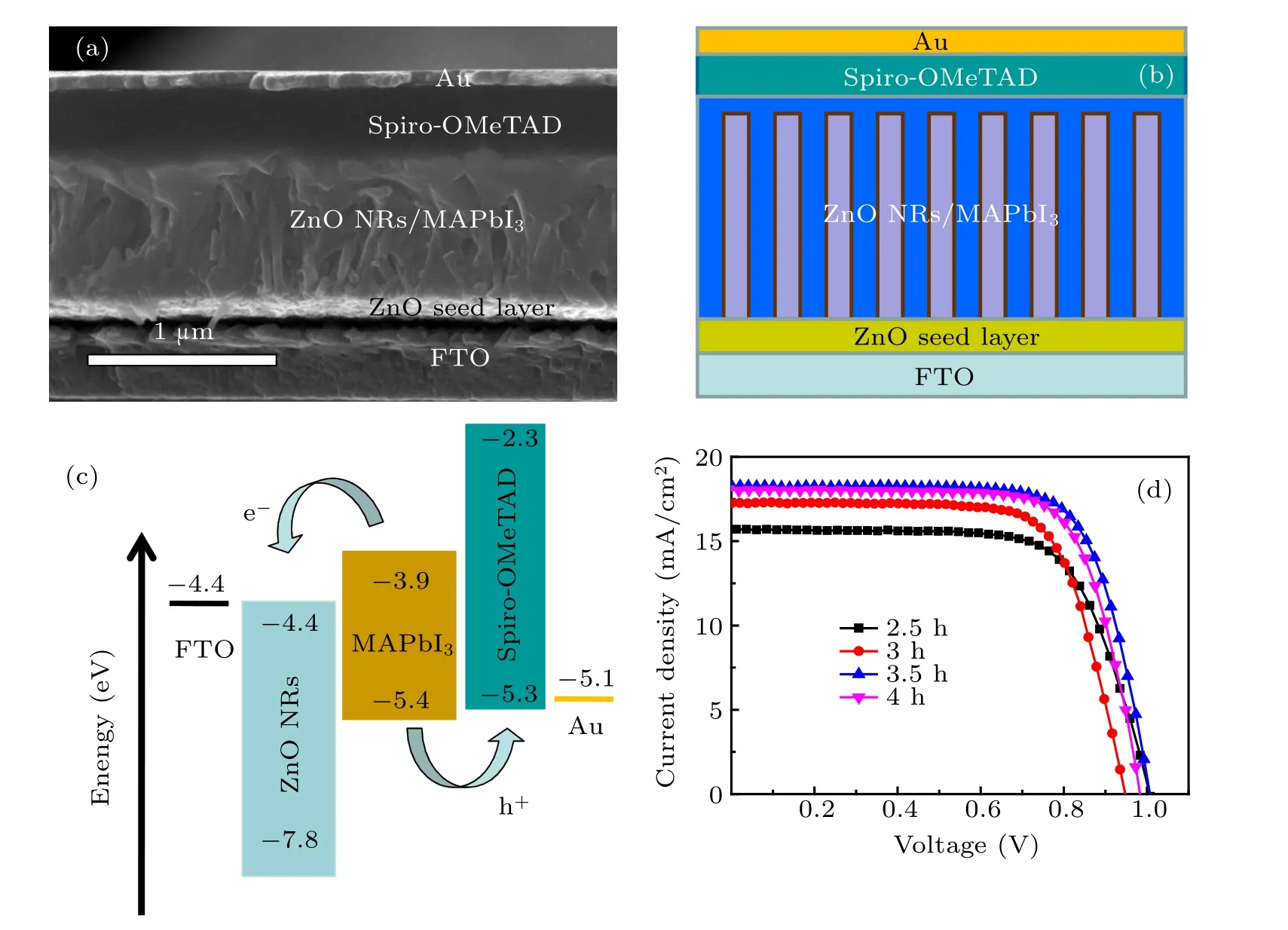
Fig.3. (a)Cross-sectional SEM images and(b)schematics of the device structure. (c)Energetic diagram of PSC based on ZnO NRs with a length of 850 nm. (d)J-V plots of the devices based on ZnO NRs with different growth time.

Fig.4. (a)Absorption spectra and(b)PL spectra of MAPbI3 film deposited on ZnO and ZnO/PVP films,(c)Nyquist plots of PSCs and(the inset depicts the equivalent circuit)(d)Mott-Schottky curves of the best devices based on ZnO and ZnO/PVP films.

Fig.5. (a)EDS elemental mapping spectra of Mg: ZnO NRs on FTO(O,Mg, and Zn). (b)XPS of Mg(5%): ZnO NRs(c)high-resolution XPS spectra of Mg 1s peak.
Mg doped ZnO NRs were prepared. Figure 5(a) shows the EDS elemental mapping of the Mg: ZnO film. The distributions of the film composition (Mg, ZnO, and O) imply Mg has been incorporated in the ZnO NRs uniformly. The existence of Mg in the film was further confirmed by the Xray photoelectron spectra(XPS)spectrum of the Mg 1s region(Figs.5(b)and 5(c)).
Figure S5 shows that the XRD patterns of the ZnO NRs with different Mg doping concentration. All the diffraction peaks correspond to the wurtzite structure of ZnO,suggesting the absence of impurity phase in the samples,and Mg doping does not alter the structure of the ZnO. We infer Mg atoms mainly exist in the ZnO as substitutes or interstitials.[31]After doping Mg, all the peaks become much stronger and sharper compared with the pristine ZnO NRs,suggesting an enhanced crystallinity of the doping ETL.[32]It is beneficial to the electron transportation and improving FF and JSCof the device performance,which will be discussed later in Fig.S6.
In order to further investigate the influence of Mg doping on the ZnO NRs, the band gap was calculated from the absorption spectra. As shown in Fig.6(a), after 5%Mg doping, the band gap increases. Based on the previous reports,the increased band gap is ascribed to the rise of the conduction band,[22,33]leading to a faster electron transportation at the interface. It is helpful to enhance the FF and JSC. Moreover,EIS measurements were performed to reveal the recombination dynamics and interfacial charge transfer of the doped and none doped PSCs. Figure 6(b)shows the Nyquist plots of the MAPbI3cells. Mg doping makes the Rrecincrease, leading to the lower carrier recombination. Rsappear to be lower than the pristine device, resulting in a faster electron injection. These results match well with the previous literature that Mg doping increased the conductivity, resulting mainly from the decreased internal resistance,which enhances the electron density in ZnO.[23]

Fig.6.(a)The extrapolated plots of(αhν)2 as a function of hν got from the absorption spectra of ZnO NRs with different content(x=0%,5%)and applied to calculate their band gaps. (b) Nyquist plots of PSCs based on ZnO NRs with different Mg content(x=0%, 5%)(the inset depicts the equivalent circuit).
Figure 7(a)depicts J-V plots of the champion PSCs based on pristine ZnO, ZnO/PVP, and ZnO: Mg (5%)/PVP layers.The performance parameters are listed in Table 1. After doping with Mg(5%),the device obtains the best PCE of 19.63%,the JSCincreases from 19.96 mA/cm2to 21.66 mA/cm2, the VOCrises from 1.13 V to 1.14 V, and the FF increases from 0.77 to 0.79. The effect of Mg doping concentration on the cells performance was also probed. The photovoltaic performance of solar cells based on the ZnO NRs with different Mg concentrations(0,1%,2%,5%,10%atomic percent)is shown in Fig.S6 and Table S3. It is clear that doping concentration significantly impacts the device performance. When the doping content increased to 10%, the photovoltaic performance of the device decreases to 15.78%, owing to a significant reduction in the JSCand FF. Obviously, 5% doping content is the optimized doping amount. With PVP coating, the performance of PSC is improved, yielding a PCE of 17.27%, the JSCincreases from 19.63 mA/cm2to 19.96 mA/cm2,the VOCand FF rise from 1.10 V to 1.13 V,0.75 to 0.77,respectively.Based on the above analysis, the obvious enhancement is ascribed to the optimized interface and the enhanced perovskite crystallinity. Both devices based on the PVP coating and the Mg doping present a higher reproducibility compared to the pristine devices(Fig.7(b)).

Table 1. Summary of device characteristics of the cells based on modified ZnO NRs under 1 sun illumination(AM 1.5G,100 mW/cm2).
The stability of PSCs based on Mg(5%): ZnO NRs with and without PVP coating were tested under lab conditions with a relative humidity of 30%-50% without encapsulation. As Fig.7(c)shows,the PCE of cell with PVP coating retains 80%of the initial PCE values after aging 30 days. While the PCE of cell without PVP coating only retains 57% after 20 days,indicating that the PVP coating contributes to the stability of the devices,which is possibly attributed to the enhanced crystallinity of MAPbI3[11]and the optimized interface.[17]

Fig.7. (a)Current density-voltage curves of devices and(b)the PCEs distribution of the devices based on ZnO NRs,ZnO/PVP,and ZnO:Mg(5%)/PVP.(c)Evolution of PCE for unsealed PSCs with or without PVP coating under lab conditions with a relative humidity of 30%-50%.
4. Conclusion
We have fabricated the effective charge collection and transportation mesoscopic perovskite solar cells based on ZnO NRs by some key optimization of the ETL and ETL/perovskite interface,comprising optimization of the preparation parameters of the ZnO NRs, the use of PVP layer, and Mg doping.The superior length of the ZnO NRs was controlled by manipulating the growth time.By inserting the PVP layer,interfacial traps were reduced, certifying by PL and EIS measurements.Meanwhile, crystallization of MAPbI3was enhanced, identified by XRD and SEM measurements. EIS measurement reveals that Mg doping increases the conductivity of ZnO NRs and improves electron extraction and transportation. Combining together, the PCE of the device rises from 16.28% to 19.63%.The devices with the PVP inserting layer also present better stability than the pristine ones. Our study provides a facile approach to improve the efficiency and the stability of photovoltaic cells. In such a synergistic way, the PSCs based on ZnO NRs are promising in the solar cell field.
猜你喜歡
Chinese Physics B(2023年2期)2023-03-13
作文小學高年級(2022年3期)2022-04-20
考試與評價·高二版(2020年6期)2020-09-10
文苑(2020年7期)2020-08-12
海峽姐妹(2019年11期)2019-12-23
作文大王·低年級(2019年2期)2019-01-23
意林(2018年19期)2018-10-31
作文大王·低年級(2018年9期)2018-10-24
課堂內外·創新作文小學版(2018年12期)2018-03-01
創新作文·低幼版(2013年1期)2013-02-04

- Chinese Physics B的其它文章
- Transport property of inhomogeneous strained graphene?
- Beam steering characteristics in high-power quantum-cascade lasers emitting at ~4.6μm?
- Multi-scale molecular dynamics simulations and applications on mechanosensitive proteins of integrins?
- Enhanced spin-orbit torque efficiency in Pt100?xNix alloy based magnetic bilayer?
- Soliton interactions and asymptotic state analysis in a discrete nonlocal nonlinear self-dual network equation of reverse-space type?
- Discontinuous event-trigger scheme for global stabilization of state-dependent switching neural networks with communication delay?