
Degradation and its fast recovery in a-IGZO thin-film transistors under negative gate bias stress*
2021-11-23 07:32JianingGuo郭佳寧DongliZhang張冬利MingxiangWang王明湘andHuaishengWang王槐生
Chinese Physics B 2021年11期
關鍵詞:王明
Jianing Guo(郭佳寧), Dongli Zhang(張冬利), Mingxiang Wang(王明湘), and Huaisheng Wang(王槐生)
School of Electronic and Information Engineering,Soochow University,Suzhou 215006,China
Keywords: amorphous IGZO,thin-film transistors,negative bias stress,subthreshold swing
1. Introduction
Amorphous InGaZnO (a-IGZO) thin-film transistors(TFTs)have attracted much attention due to the characteristics including high electron mobility, low leakage current, small subthreshold swing, and high large-area uniformity. a-IGZO TFTs with a back-channel etching (BCE) structure have no protection at the back channel. Thus, the back channel may be damaged during the patterning of the source/drain electrodes,and the device performance becomes deteriorated.[1]In the etching-stop layer(ESL)structure,a dielectric layer is deposited to protect the back channel. However,an extra mask is required to pattern the ESL,which increases the process complexity. The ESL also increases the characteristic size of the device. Elevated-metal metal-oxide(EMMO)TFT makes up for the shortcomings of traditional BCE and ESL TFTs by elevating the source/drain electrodes above the passivation layer and the formation of conductive source/drain regions.[2,3]
In this paper,positive shift of the transfer curve and severe degradation in the subthreshold characteristics were observed for a-IGZO TFTs under NBS and NBIS, and a gentle degradation is observed under PBS and PBIS. A fast recovery of the degradation in the threshold voltage(VTH)and subthreshold swing (SS) is observed for the a-IGZO TFTs under NBS and NBIS,and no degradation can be observed when the transfer curves are measured with gate bias sweeping from positive gate bias to negative gate bias direction. The mechanisms for the degradation and its recovery under gate bias stress with or without illuminations are proposed.
2. Experiments
As shown in Fig. 1, the a-IGZO TFTs with an EMMO structure were fabricated and used. A 300-nm thick Mo was sputtered and patterned as the gate electrode. The gate insulator consists of 50-nm silicon nitride (SiNx) and 75-nm silicon dioxide (SiOx), deposited by plasma-enhanced chemical vapor deposition (PECVD). A two-hour annealing at 400°C was performed in O2to remove the residual hydrogen in the gate insulator. Then, a 20-nm a-IGZO was sputtered at room temperature as the active layer. The passivation layer is 300-nm SiOxdeposited by PECVD,and another dehydrogenation treatment was performed in O2for two hours. After metallization, a critical oxidizing heat treatment was performed at 400°C for two hours to form the low-resistance source/drain regions.
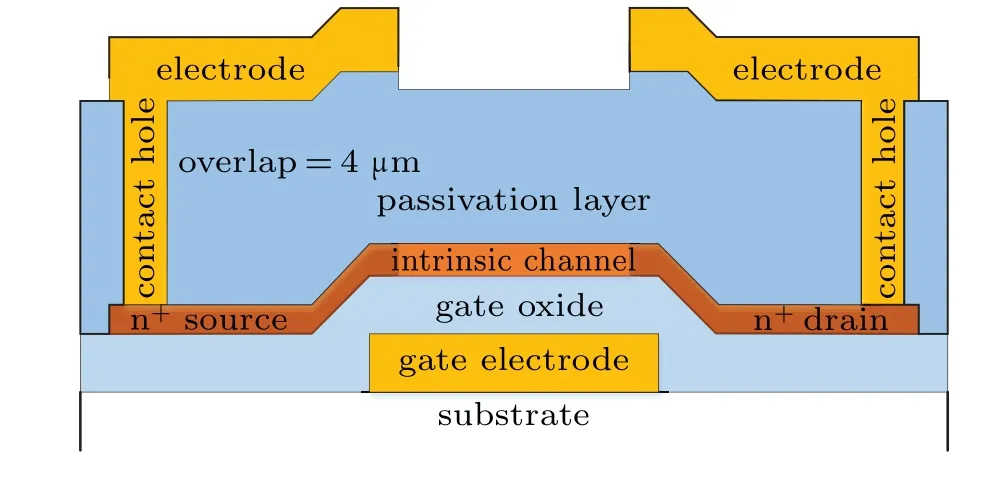
Fig.1. Schematic cross-sectional diagram of the EMMO-type a-IGZO TFT.
For the reliability experiments under gate bias stress,the source/drain electrodes were grounded and the gate electrodes was applied with a bias of?20 V or 20 V. Illumination is applied with LED monochromatic light sources with wavelengths of 660 nm(red), 520 nm(green), and 445 nm(blue).The transfer curves of the TFTs before and after stress were measured with Agilent 4156C semiconductor parameter analyzer,and the transfer curves before and after NBIS and PBIS were measured under illumination. The channel width and length of a-IGZO TFTs are 50 μm and 20 μm, respectively,and the overlap between the gate and source/drain electrodes is 4μm.VTHis estimated by the linear extrapolation method from the transfer curve atVdsof 0.1 V. The flat-band voltage(VFB)is defined as the gate voltage at which drain current begins to transit to the subthreshold region.
3. Results and discussion
3.1. NBS and NBIS degradation
As shown in Fig.2(a),the transfer curve shows an evident degradation in the subthreshold swing and threshold voltage after NBS with a gate voltage of?20 V.The variations ofVTH(?VTH) andSS(?SS) are extracted and plottedversusstress time in Fig.3.VTH,VFB,andSSbehave differently with stress time,whereVTHinitially exhibits an evident positive shift after 10 s and continues to gradually shift toward positive gate bias direction with the increase in stress time,SSincreases significantly after 10-s stress time, but it remains almost unchanged during the following stress period. However,VFBincreases continually with the increase in stress time. This rapid degradation ofVTHhas also been observed in previous studies,where theVTHshifts toward negative gate bias direction rather than positive gate bias direction.[12]The degradations inVTH,VFB,andSScan be recovered,but the corresponding recovery also behaves differently.One can notice from Fig.2(b)that the degradation inSSrecovers fast in the first 10 s after the stress is removed and gradually recovers completely in 1800 s.VFBrecovers completely in 10 s butVTHrecovers more slowly.

Fig.2. Evolutions of the transfer curves in linear and logarithmic scales for the TFTs(a)under NBS and(b)after NBS is removed.

whereCoxis the oxide capacitance per unit area,qis the elementary charge,kBis the Boltzmann constant, andTis the absolute temperature. In a-IGZO, singly charged oxygen vacancies (V+o) are the main type of deep states,[13]which is a metastable state and can explain the fast recovery of theSSafter stress. The increased deep states can also trap parts of the accumulated carriers and increase the threshold voltage.

Fig.3. (a)?VTH and ?SS under NBS and NBIS with the stress time and(b)with the recovery time after the stress is removed.

Fig.4. Evolution of the transfer curves in linear and logarithmic scales for the TFTs(a)under NBIS and(b)after NBIS is removed.
Figure 4(a) shows that the degradation phenomena of NBIS with blue light of a power density(IL)of 2 mW/cm2are similar to those under NBS,i.e.,SSandVTHare increased.The slope of transfer curve in on-state is also increased. But differently,no evident positive shift ofVFBis found under NBIS.Furthermore, as shown in Fig. 4(b),VFBinitially exhibits a negative shift and then recovers to its initial values after the NBIS is removed. For the first time such type of recovery phenomenon has been reported.
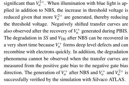
NBIS usually introduces more severe degradation than NBS due to the ionization of neutral oxygen vacancies under illumination.[9,13]However, after comparing the degradation and recovery ofSSandVTHunder NBS and NBIS, as shown in Fig. 3, the shift ofVTHunder NBIS is found to be smaller than that under NBS. Thus, two degradation mechanisms involved under NBIS are proposed. One mechanism is caused by the negative gate bias, and the corresponding degradation is similar to that under NBS.The features include increase inSS,VTH,andVFBand their recovery in a short time. The other mechanism causes negative shift inVFBandVTH, resulting in the smaller shift ofVFBandVTHunder NBIS than that under NBS.Moreover,the a-IGZO TFT after NBIS shows a negative shift ofVFBafter the rapid recovery of the on-state characteristics.
The dependence of ?VTHon stress time after NBS and NBIS was fitted with the stretched exponential function, as follows:
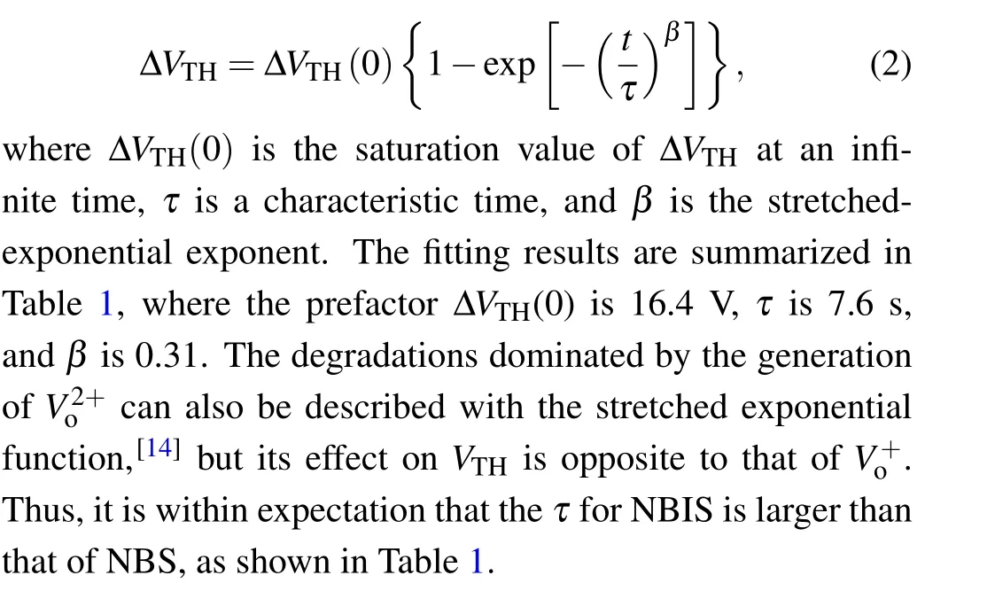

Table 1. Fitting parameters for the fitting of the dependence of ?VTH onstress time after NBS and NBIS with the stretched exponential function.
To clarify the degradation mechanism, which causes the negative shift ofVFBafter the removal of NBIS,the degradation of a-IGZO TFT under illumination stress only was further investigated. As shown in Fig. 5, under the illumination of blue light with a power density of 2 mW/cm2, only a small amount of increase in the on-state current (Ion) is found, and the increase inIondoes not increase with the increase in stress time. Thus,the increase inIonunder illumination is proposed due to the photo generated carriers.[15]Then,the negative shift ofVFBafter NBIS should be caused by the combination of the


Fig.5. Evolution of the transfer curves in linear and logarithmic scales for the TFTs under illumination with blue light.
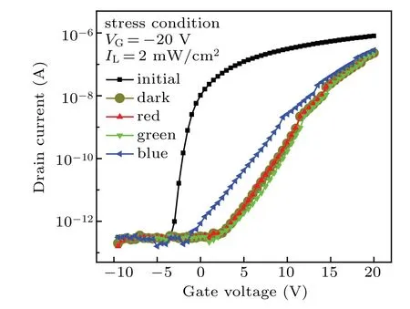
Fig. 6. Comparison of the transfer curves of the a-IGZO TFTs before and after NBIS with the light of different wavelengths.

3.2. PBS and PBIS degradation


Fig.7. Evolution of the transfer curves in linear and logarithmic scales for the TFTs(a)under PBS and(b)after PBS is removed.


Fig.8. Evolution of the transfer curves in linear and logarithmic scales for scales the TFTs(a)under PBIS and(b)after PBIS is removed.

Fig.9.VFB and SS at the initial,after stress for 1000 s and 60 s and 24 h after the stress is removed for the cases of(a)PBS and(b)PBIS.
3.3. Degradation mechanism with V+o
Therefore,the introduction ofV+ois the dominant degradation mechanism under NBS and a small amount ofV+ocan also be induced under PBIS. They can be explained with the band diagrams shown in Fig.10. When a negative gate bias is applied, the energy band is bent upward, and the Fermi level is close to the valance band at the channel surface. Electrons at the trap states of neutral oxygen vacancies higher than the Fermi level are emitted,and the neutral oxygen vacancies are ionized intoV+oandV2+o, which are distributed as deep trap states and shallow trap states in the bandgap,respectively.V+oresults in the degradation ofSSand the increase inVTHandVFB. The number ofV2+ois relatively small, such that its effect is minimal. Moreover,V+ois metastable and easy to recombine with electrons, so the degradation recovers quickly after removing the stress.It is speculated that nitrogen is introduced into the channel a-IGZO from the gate dielectric during the annealing processes for dehydrogenation and formation of source/drain. They can form Zn=N bonds with one Zn atom at an oxygen vacancy site and the other Zn atom then tends to formV+owhen it is ionized.[20]
When a positive gate voltage is applied after NBS,highconcentration electrons accumulate at the channel surface,and the accumulatedV+ocan recombine with electrons more quickly. This recovery process requires only a few milliseconds.[21]Thus,when the transfer curve is measured with sufficiently high positive gate voltages,the current exhibits a steplike rise and the slopes of the curves of the on-state region rises,as shown in Figs.2 and 4. This finding can also explain the phenomenon that the degradation in the subthreshold region cannot be observed, when the transfer curve after NBS is measured with the gate voltage sweeping from positive gate bias to the negative gate bias direction, as shown in Fig. 11.This condition may also be the reason why degradation in the subthreshold swing was seldom observed and reported in the literature. For the increasedafter a longer stress time,the unrecombinedunder a positive gate bias can minimally decrease the on-state current.
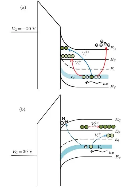
Fig.10.Schematic energy band diagrams showing the generation ofandunder(a)NBIS and(b)PBIS.


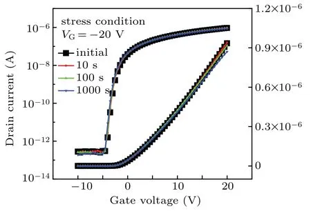
Fig.11. Evolution of the transfer curves in linear and logarithmic scales for the TFTs under NBS measured from positive gate voltage to negative gate voltage.
3.4. Simulation verification

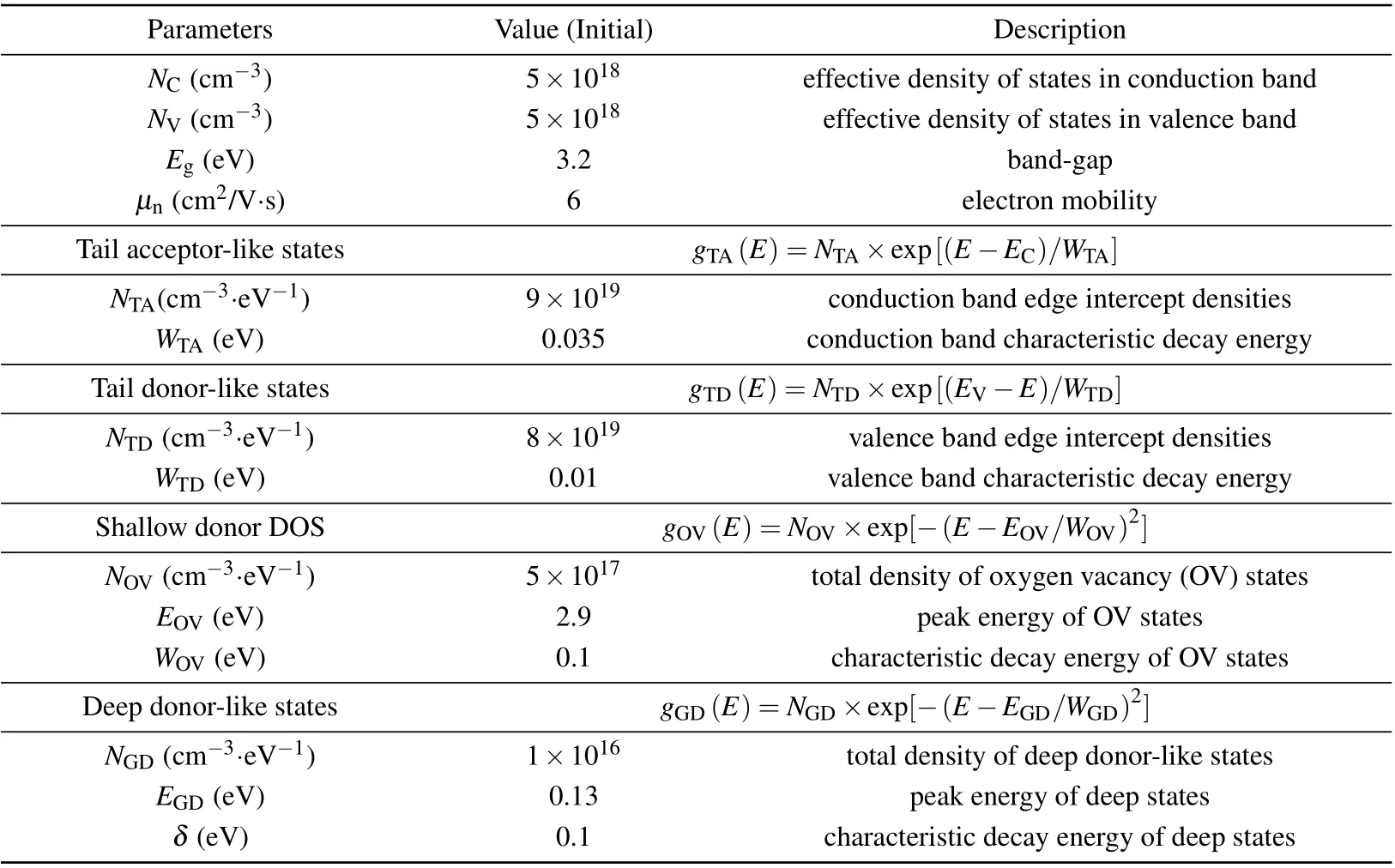
Table 2. Parameters for the simulation of the initial transfer curves of the initial a-IGZO TFT.

Table 3. Parameters for the DOS added during the simulation of the transfer curves after stress.
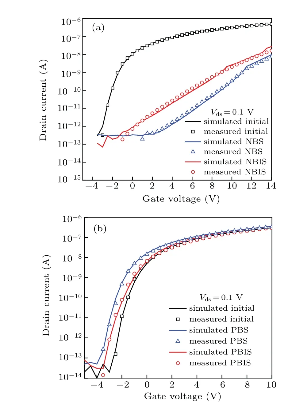
Fig.12. Comparison of the measured and simulated transfer curves for the a-IGZO TFTs after (a) NBS and NBIS and (b) PBS and PBIS for 1000 s.The initial transfer curves are added for reference.

Fig.13. Comparison of the DOS extracted after simulation for(a)the initial TFT and the TFT after NBS and NBIS for 1000 s, and (b) the initial TFT and the TFT after PBS and PBIS for 1000 s.
4. Conclusions
Increased threshold voltage and deteriorated subthreshold characteristics of a-IGZO TFTs after NBS are observed and proposed to be due to the generation ofV+o, which is more
猜你喜歡
Chinese Physics B(2022年12期)2022-12-28
Chinese Physics B(2022年8期)2022-08-31
應用數學(2022年3期)2022-07-07
北方音樂(2019年10期)2019-07-10
北方音樂(2019年10期)2019-07-10
海峽姐妹(2019年3期)2019-06-18
金色年華(2017年2期)2017-06-15
棋藝(2014年1期)2014-05-20
- Chinese Physics B的其它文章
- Numerical investigation on threading dislocation bending with InAs/GaAs quantum dots*
- Connes distance of 2D harmonic oscillators in quantum phase space*
- Effect of external electric field on the terahertz transmission characteristics of electrolyte solutions*
- Classical-field description of Bose-Einstein condensation of parallel light in a nonlinear optical cavity*
- Dense coding capacity in correlated noisy channels with weak measurement*
- Probability density and oscillating period of magnetopolaron in parabolic quantum dot in the presence of Rashba effect and temperature*