
Mode characteristics of nested eccentric waveguides constructed by two cylindrical nanowires coated with graphene
2022-03-12 07:49JiLiu劉吉LixiaYu于麗霞andWenruiXue薛文瑞
Chinese Physics B 2022年3期
Ji Liu(劉吉) Lixia Yu(于麗霞) and Wenrui Xue(薛文瑞)
1Key Laboratory of Instrumentation Science and Dynamic Measurement of Ministry of Education,North University of China,Taiyuan 030051,China
2School of Information and Communication Engineering,North University of China,Taiyuan 030051,China 3College of Physics and Electronic Engineering,Shanxi University,Taiyuan 030006,China
Keywords: graphene,nanowire,waveguide,multipole method
1. Introduction
Surface plasmon waveguides (SPWs) are a new type of waveguide, which uses surface plasmon polaritons(SPPs)[1]to guide the transmission of electromagnetic waves.The main materials used in SPWs are noble metals,[2]semiconductors,[3]graphene,[4]etc. The size of these waveguides is in micron or nanometer scale, and they are expected to be widely used in highly integrated photonic chips[5]and in the field of sensing.[6]Graphene is a new type of two-dimensional material, which has been applied in many fields.[7-9]Compared to conventional metal materials (e.g., silver and gold), graphene has desirable properties, such as tunability, extreme confinement, crystallinity and low loss. Because of these unique properties, graphene has been recently proposed as a platform for plasmon waveguiding from THz to infrared frequencies.[10]By coating single[11,12]or multi-layer[13-15]graphene on the surface of dielectrics,strip,[16-18]circular,[11,12]elliptical[19]and hybrid[20-26]SPWs can be formed. On this basis, parallel SPWs can be constructed.[27-29]
The nested surface plasmon waveguide coated with graphene is a research hotspot. In 2015, Yanget al.designed a circular dielectric nanowire waveguide coated with two layers of graphene,[13]which can be regarded as a coaxial waveguide formed by embedding one graphene-coated dielectric nanowire into the axis of the other. By solving the dispersion equation, it is found that the Fermi energy of graphene,the distance between the two layers of graphene and the radius of the waveguide can affect the behavior of the modes supported by the waveguide. The nested surface plasmon waveguide designed by Liuet al.in 2017 can be regarded as a coaxial waveguide formed by embedding a graphene-coated cylindrical silicon nanowire into the axis of another graphenecoated cylindrical silicon dioxide nanowire.[14]The results show that the fundamental mode supported by the waveguide has a longer propagation distance and a smaller mode area.In 2017, Xinget al.designed a circular dielectric nanowire waveguide coated with multilayer graphene,[15]which can be regarded as a coaxial waveguide formed by embedding multiple graphene-coated dielectric nanowires with a gradually decreasing radius into the axis of graphene-coated dielectric nanowires with a larger radius. The results show that the waveguide has a strong ability to confine the field, and the mode characteristics can be adjusted by the chemical potential of graphene. In 2019, Chenget al.designed a graphene coated confocal elliptical dielectric nanowire waveguide,[19]which can be regarded as a waveguide formed by embedding one elliptical dielectric nanowire into another and keeping the two elliptical dielectric nanowires confocal. The results show that, compared with the elliptical dielectric nanowire waveguide coated with single-layer graphene,this kind of waveguide has better mode performance and a wider adjustable range.Since a common feature of the above waveguides is that the embedded waveguide and parent waveguide have the same axis of symmetry,the components of the field can be expanded in the same coordinate system when studying the mode characteristics. Based on the boundary conditions, the dispersion equation is obtained, and then the effective refractive index and field distribution are obtained.If the embedded waveguide is eccentric, this method will not work and the mode characteristics of the waveguide will not be obtained.
In this paper, the mode characteristics of a kind of graphene-coated cylindrical dielectric nanowire waveguide embedded with eccentric cylindrical dielectric nanowire are studied using the multipole method.[30]This method can effectively overcome the difficulties mentioned above. To verify the obtained results, the FEM method is used. This paper is structured as follows. Section 2 gives the theoretical model.Section 3 presents the result and discussion. The last section is the conclusion.
2. Theoretical model
The waveguide structure designed in this paper is shown in Fig. 1. It consists of a circular parent dielectric nanowire(wire 2)with a radius ofρ20and a circular embedded dielectric nanowire (wire 1) with a radius ofρ10. Wire 1 and wire 2 are eccentric. The minimum spacing between the outer surface of wire 1 and the inner surface of wire 2 iss. Suppose that the dielectric constant of wire 1 isε1(region I), wire 2 isε2(region II) and the background isε3(region III). The surface of wire 1 and wire 2 is coated with a single layer of graphene. The conductivity of graphene,σg, has been computed within the random-phase approximation.[31]This kind of waveguide structure may be successfully fabricated using the preform-drawing method[32]and chemical vapor deposition(CVD)method.[33]

Fig. 1. Crosssection of the waveguide composed of one circular parent dielectric nanowire coated with graphene and one circular embedded dielectric nanowire coated with graphene.
As shown in Fig.1,the rectangular coordinate systemo1-x1y1z1and the cylindrical coordinate systemo1-ρ1φ1z1are established with the symmetrical center of wire 1 as the coordinate origin. The rectangular coordinate systemo2-x2y2z2,o-xyzand the cylindrical coordinate systemo2-ρ2φ2z2are established with the symmetrical center of wire 2 as the coordinate origin. According to the multipole method,[30]assuming that wire 1 and wire 2 exist separately, theEzandHzfields inside and outside the wire are distributed as follows in their respective coordinate systems:
Inside wire 1:

Graphene is regarded as a material with zero thickness and conductivityσg.At the interface of regions I,II and III,the following relation of the boundary value of tangential fields can be applied:

According to Eqs. (18)-(25), a set of linear algebraic equations can be obtained by using the point by point matching method[37]on the interface:

The linear algebraic Eq. (26) is solved by our own Fortran 90 program. The distribution of field, the real part Re(neff)and the imaginary part Im(neff) of the effective refractive index of each mode can be obtained. The propagation length is given by the formulaLprop=λ/[4πIm(neff)].[38,39]The figure of merit is given by FoM=Re(neff)/Im(neff),[39]which can be used to characterize the transmission performance of the waveguide.
3. Results and discussion
3.1. Classification of modes
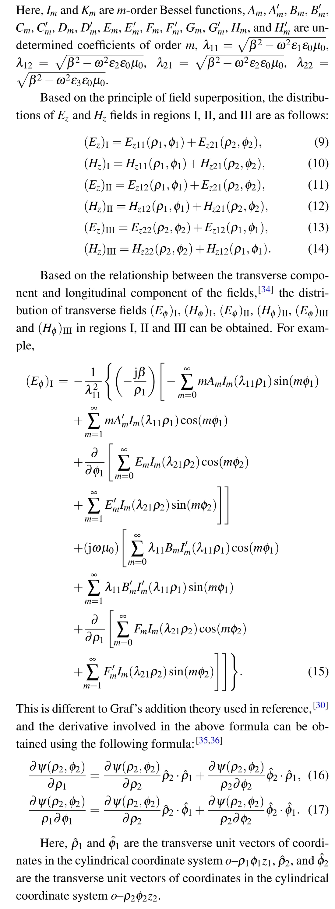
Table 1 shows the combination of the three lowest-order modes supported by the waveguide, the distribution of the electric field component in thezdirection and the distribution of the electric field intensity under the conditions ofλ=7 μm,Ef=0.5 eV,ρ10=75 nm,ρ20=150 nm,s=20 nm,ε1=1.0,ε2=2.1025,andε3=1.0. The three modes are named mode 0, mode 1 and mode 2 in turn. Mode 0 is combined by zeroorder modes of the two single rods, and the electric field is mainly distributed in the gap region between the two layers of graphene on the right side of the waveguide. Mode 1 and mode 2 are combined by the first-order modes of two single
rods. Thezcomponent of the electric field of mode 1 is antisymmetric about the horizontal axis, and thezcomponent of the electric field of mode 2 is symmetric about the horizontal axis.
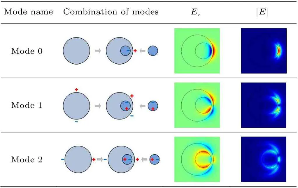
Table 1. The combination of the three lowest-order modes supported by the waveguide, the distribution of the electric field component in the z direction and the distribution of the electric field intensity under the conditions of λ =7 μm, Ef =0.5 eV,ρ10 =75 nm, ρ20 =150 nm, s=20 nm, ε1 =1.0,ε2=2.1025,and ε3=1.0.
3.2. Influence of working wavelength on transmission characteristics
SettingEf=0.5 eV,ρ10=75 nm,ρ20=150 nm,s=20 nm,ε1=1.0,ε2=2.1025, andε3=1.0, the relationship between Re(neff),Lprop, and FoM of the three lowest-order modes and the working wavelengthλis shown in Figs.2(a)-2(c). In these figures,the solid line is the result obtained using the FEM method,and the solid point line is the result obtained using the multipole method. If there is no special explanation,this marking method will be used in the following. With typical parameters,the conductivity of graphene varies greatly in the frequency range of 10 THz-100 THz, especially in the range of 40 THz-50 THz, and the corresponding wavelength range is about 6 μm-8 μm.[40]When the operating wavelength increases from 6.00 μm to 8.00 μm, the Re(neff)-curves of the three lowest-order modes decrease monotonously and the distance between these curves increases. TheLprop-curves increase monotonically. TheLprop-curve of mode 2 intersects with theLprop-curve of mode 0 at 7.00 μm,and intersects with theLprop-curve of mode 1 at 7.00 μm. The FoM-curve corresponding to mode 0 increases gradually,and the FoM value of mode 1 and mode 2 reaches a peak at 7.0 μm and then decreases gradually. In the selected parameter range, mode 0 has the highest figure of merit and the best performance. The two embedded graphs in Fig. 2(b) show the field distribution of mode 0 when the operating wavelengths are 6.0 μm and 8.0 μm.Comparing the two embedded graphs,we can see that when the wavelength is short, the field distribution is mainly concentrated near the inner and outer graphene layers,and the electric field intensity is the largest near the inner graphene layer, and the interaction between the field and graphene is the largest. In addition, the waveguide loss is larger and the propagation length is shorter. When the wavelength is longer,the electric field diffuses to the dielectric layer between the two layers of graphene, the confinement of the waveguide to the field is weakened,the loss is reduced and the propagation length is longer.
Fig.2.The relationship between Re(neff),Lprop,and FoM of the three lowestorder modes and the working wavelength λ when Ef=0.5 eV,ρ10=75 nm,ρ20=150 nm,s=20 nm,ε1=1.0,ε2=2.1025,and ε3=1.0.
3.3. Influence of the radius of wire 1 on transmission characteristics

Fig.3.The relationship between Re(neff),Lprop,and FoM of the three lowestorder modes and the radius ρ10 of wire 1 when λ =7.0 μm, Ef =0.5 eV,ρ20=150 nm,s=20 nm,ε1=1.0,ε2=2.1025,and ε3=1.0.
Settingλ=7 μm,Ef=0.5 eV,ρ20=150 nm,s=20 nm,ε1=1.0,ε2=2.1025,andε3=1.0,the relationship between Re(neff),Lpropand FoM of the three lowest-order modes and the radiusρ10of wire 1 is shown in Figs. 3(a)-3(c). As the radius of the inner wireρ10increases gradually, the real part trates to the region between the two layers of graphene. Whenρ10=65 nm, the field distribution decreases, the field intensity is not very strong and the interaction between the field and graphene is the smallest. Furthermore, the waveguide loss is the smallest and the propagation length is the longest. Whenρ10=100 nm, the field is mainly concentrated between the inner and outer graphene layers on the right side of the waveguide. The field intensity is higher and the interaction between the field and graphene becomes larger. In addition,the waveguide loss becomes larger and the propagation length becomes shorter.of the effective refractive index Re(neff) of mode 0, mode 1 and mode 2 increase monotonically. TheLpropof mode 0 and mode 1 increase slowly and monotonically, while theLpropof mode 2 increases gradually at first, reaches maximum at 65 nm,and then decreases gradually. In the selected parameter range, mode 0 has the highest figure of merit and the best performance. The three embedded graphs in Fig. 3(b) show the field distribution of mode 2 when the radius of the inner wireρ10is 50 nm, 65 nm, and 100 nm. Comparing the three embedded graphs, we can see that whenρ10=50 nm,the field is widely distributed on the inner and outer graphene layers, and the interaction between the field and graphene is large. In addition, the waveguide loss is large and the propagation length is short. Whenρ10increases gradually,the field shifts to the right side of the waveguide and gradually concen-

Fig. 4. The dependence of Re(neff), Lprop, and FoM of the three lowestorder modes on the radius ρ20 of wire 2 when λ =7.0 μm, Ef =0.5 eV,ρ10=75 nm,s=20 nm,ε1=1.0,ε2=2.1025,and ε3=1.0.
3.4. Influence of the radius of wire 2 on transmission characteristics
Settingλ=7 μm,Ef=0.5 eV,ρ10=75 nm,s=20 nm,ε1= 1.0,ε2= 2.1025, andε3= 1.0, the dependence of Re(neff),Lprop, and FoM of the three lowest-order modes on the radiusρ20of wire 2 is shown in Figs. 4(a)-4(c). When the radiusρ20of the outer wire is increased, the real part of the effective index of mode 0,mode 1 and mode 2 monotonically decreases,and the distance between the curves increases.The propagation length of the three modes decreases slowly,but the change is not significant. In the selected parameter range,mode 0 has the highest figure of merit and the best performance. The two images embedded in Fig. 4(b) show the field distribution map corresponding to mode 0 whenρ20is 100 nm and 200 nm,respectively. Comparing the two embedded images, we can see that the field is concentrated in the area near the inner and outer graphene layers on the right side of the waveguide. Whenρ20=100 nm,the distribution range of the field is large,but the intensity of the field is weak.Whenρ20=200 nm,the distribution range of the field is small,but the intensity of the field is strong.In both cases,the interaction strength between the field and graphene is close, the waveguide loss is close and the propagation length is also close.
3.5. Influence of the minimum spacing on transmission characteristics
Settingλ= 7 μm,Ef= 0.5 eV,ρ10= 75 nm,ρ20=150 nm,ε1=1.0,ε2=2.1025,andε3=1.0,the dependence of Re(neff),Lprop,and FoM of the three lowest-order modes on the minimum spacing between the inner and outer cylinderssare shown in Figs.5(a)-5(c). Increasing the minimum spacing between the inner and outer cylinders,the real part of the effective index of the three modes monotonically decreases,and the spacing between the curves becomes smaller.The propagation lengths of the three modes increase monotonously, the curve corresponding to mode 0 increases faster than that corresponding to mode 1, and the curve corresponding to mode 2 intersects with the other two curves.The transmission performance of mode 0 and mode 1 decreases,while the transmission performance of mode 2 is almost unaffected. The two embedded images in Fig.5(b)show that the field distribution of mode 0 corresponding tosis 10 nm and 30 nm,respectively. Comparing the two embedded images,we can see that when the minimum spacing between the inner and outer cylinders is small,the area of field distribution is small,the field intensity is high,the confinement of the waveguide to the field is strong,the interaction between the field and graphene is strong,the waveguide loss is large and the propagation length is short. When the minimum spacing between the inner and outer cylinders is large,the area of field distribution is large,the field strength is weak, the confinement of the waveguide to the field is weak,the interaction between the field and graphene is weak, the waveguide loss is small and the propagation length is long.

Fig.5. The dependence of Re(neff),Lprop,and FoM of the three lowest-order modes on the minimum spacing between the inner and outer cylinders s when λ =7.0, Ef =0.5 eV, ρ10 =75 nm, ρ20 =150 nm, ε1 =1.0, ε2 =2.1025 and ε3=1.0.
3.6. Influence of the Fermi energy on transmission characteristics
Settingλ= 7 μm,ρ10= 75 nm,ρ20= 150 nm,s= 20 nm,ε1= 1.0,ε2= 2.1025, andε3= 1.0, the dependence of Re(neff),Lprop, and FoM of the three lowestorder modes on the Fermi energyEfis shown in Figs. 6(a)-6(c). With the increase inEf, the real part of the effective refractive index of the three lowest-order modes decreases monotonously, the confinement of the waveguide to the field decreases, the interaction between the field and graphene weakens, the loss decreases and the propagation length increases. In this changing process, the propagation length of the three modes shows little difference.When the Fermi energy of graphene increases from 0.2 eV to the dielectric layer between the two layers of graphene,the field strength on the graphene is weak,the confinement of the waveguide to the field is weak, the interaction between the field and graphene is weak, the waveguide loss is small and the propagation length is long.to 0.8 eV,the propagation length of mode 2 will gradually exceed the other two modes. Mode 0 always leads the other two modes with a higher figure of merit. By adjusting the Fermi level of graphene,the mode transmission performance can be improved obviously. The two embedded images in Fig. 6(b)show the field distribution of mode 0 whenEfis 0.2 eV and 0.8 eV, respectively. Comparing the two embedded images,we can see that when the Fermi energy of graphene is small,the field distribution is mainly confined to the inner and outer graphene layers, the intensity of the field on the graphene is high, the confinement of the waveguide to the field is strong,the interaction between the field and graphene is strong, the waveguide loss is large and the propagation length is short.When the Fermi energy of graphene is large,the field diffuses

Fig.6. The dependence of Re(neff),Lprop,and FoM of the three lowestorder modes on the Fermi energy Ef when λ=7.0 μm,ρ10=75 nm,ρ20=150 nm,s=20 nm,ε1=1.0,ε2=2.1025,and ε3=1.0.

Fig.7. The dependence of Re(neff),Lprop and FoM of the three lowestorder modes on the dielectric constant of region I ε1 when λ=7.0 μm,Ef=0.5 eV,ρ10=75 nm,ρ20=150 nm,s=20 nm,ε2=2.1025,and ε3=1.0.
3.7. Influence of the dielectric constant of region I on transmission characteristics
Settingλ= 7 μm,Ef= 0.5 eV,ρ10= 75 nm,ρ20=150 nm,s=20 nm,ε2=2.1025, andε3=1.0, the dependence of Re(neff),Lprop, and FoM of the three lowest-order modes on the dielectric constant of region Iε1is shown in Figs. 7(a)-7(c). With the increase inε1, the real parts of the effective refractive index of the three lowest-order modes increase monotonically,the confinement of the waveguide to the field becomes stronger, the interaction between the field and graphene becomes stronger, the loss increases, the propagation length decreases monotonously and the quality factor of the mode decreases gradually. The two embedded images in Fig.7(b)show the field distribution of mode 0 whenε1is 1.0 and 3.0, respectively. Comparing the two embedded images,we can see that when the dielectric constant of region I is small,the field intensity,the confinement of the waveguide to the field and the interaction between the field and graphene are weak. In addition,the waveguide loss is small and the propagation length is long. In contrast,when the dielectric constant of region I is large, the field intensity, the confinement of the waveguide to the field and the interaction between the field and graphene are strong, the waveguide loss is large and the propagation length is short.

Fig. 8. The dependence of Re(neff), Lprop, and FoM of the three lowestorder modes on the dielectric constant of region III ε3 when λ =7.0 μm,Ef = 0.5 eV, ρ10 = 75 nm, ρ20 = 150 nm, s = 20 nm, ε1 = 1.0, and ε2=2.1025.
3.8. Influence of the dielectric constant of region III on transmission characteristics
Settingλ= 7 μm,Ef= 0.5 eV,ρ10= 75 nm,ρ20=150 nm,s=20 nm,ε1=1.0, andε2=2.1025, the dependence of Re(neff),Lprop, and FoM of the three lowest-order modes on the dielectric constant of region IIIε3is shown in Figs. 8(a)-8(c). Increasingε3, the real parts of the effective refractive index of the three lowest-order modes increase monotonically, and the confinement of the waveguide to the field becomes stronger. The interaction between the field and graphene becomes stronger, the loss increases, the propagation length decreases monotonously,and the figure of merit of the mode decreases gradually. The two embedded images in Fig.8(b)show the field distribution of mode 0 whenε3is 1.0 and 3.0, respectively. Comparing the two embedded images,we can see that when the dielectric constant of region III is small, the intensity of the field is weak, the confinement of the waveguide to the field is weak,the interaction between the field and graphene is weak, the waveguide loss is small and the propagation length is long. When the permittivity of region III is large, the field intensity is strong, the confinement of the waveguide to the field is strong,the interaction between the field and graphene is strong, the waveguide loss is large and the propagation length is short.
4. Conclusion
The multipole method can effectively solve the mode problem of the graphene coated nested dielectric waveguide.Mode 0 is combined by the zero-order modes of two single nanowires.Mode 1 and mode 2 are combined by the first-order modes of two single nanowires. Within the selected parameter range, we find that mode 0 has the highest quality factor and the best performance. As the wavelength,the minimum spacing between the inner and the outer cylinders,the radius of the inner cylinder and the Fermi energy of graphene increase,the confinement of the waveguide to the three lowest-order modes decreases, the loss decreases and the propagation length increases. When the radius of the outer cylinder, the dielectric constant of region I or the dielectric constant of region III increases,the confinement of the waveguide to the three lowestorder modes increases,the loss increases and the propagation length decreases. These results have been verified by the FEM method. This work has provided a theoretical basis for the design,fabrication and application of nested dielectric nanowire waveguides coated with graphene.
Acknowledgments
Project supported by the Natural Science Foundation of Shanxi Province, China (Grant Nos. 201901D111159 and 2021D20021310) and the Shanxi Scholarship Council of China(Grant No.HGKY2019068).

- Chinese Physics B的其它文章
- Measurements of the 107Ag neutron capture cross sections with pulse height weighting technique at the CSNS Back-n facility
- Measuring Loschmidt echo via Floquet engineering in superconducting circuits
- Electronic structure and spin-orbit coupling in ternary transition metal chalcogenides Cu2TlX2(X =Se,Te)
- Characterization of the N-polar GaN film grown on C-plane sapphire and misoriented C-plane sapphire substrates by MOCVD
- Review on typical applications and computational optimizations based on semiclassical methods in strong-field physics
- Quantum partial least squares regression algorithm for multiple correlation problem