
Magnetic proximity effect induced spin splitting in two-dimensional antimonene/Fe3GeTe2 van der Waals heterostructures
2022-03-12 07:49XiuyaSu蘇秀崖HelinQin秦河林ZhongboYan嚴忠波DingyongZhong鐘定永andDonghuiGuo郭東輝
Chinese Physics B 2022年3期
Xiuya Su(蘇秀崖) Helin Qin(秦河林) Zhongbo Yan(嚴忠波)Dingyong Zhong(鐘定永) and Donghui Guo(郭東輝)
1School of Physics,Sun Yat-sen University,Guangzhou 510275,China
2State Key Laboratory of Optoelectronic Materials and Technologies,Sun Yat-sen University,Guangzhou 510275,China
Keywords: first-principles calculations,antimonene/Fe3GeTe2 vdW heterostructures,magnetic proximity effect,spin splitting
1. Introduction
Proximity effects offer fascinating opportunities for tailoring the band structures of adjacent materials.[1-3]In particular,magnetic proximity effect is an important method for introducing magnetism into non-magnetic materials and inducing novel properties.[4-6]Recently,magnetic proximity effect has been used to create Majorana states in a superconducting/ferromagnetic hybrid system.[7]Besides, magnetic proximity effect can induce spin splitting owing to the local magnetic exchange field, which has a short-range nature without significantly altering the overall band structures.[8]
Magnetic proximity effect in two-dimensional (2D) van der Waals (vdW) magnetic heterostructures has been investigated theoretically and experimentally.[9]Owing to the weak interlayer coupling in vdW heterostructures,the primary properties of each component can be retained while novel features may also be produced.For instance,it has been experimentally confirmed that by integrating graphene with CrBr3to construct vdW heterostructures, a certain degree of magnetism can be introduced into graphene.[4]Zollner’s group has reported that magnetic proximity effect in MoSe2/CrI3and WSe2/CrI3heterostructures can be modulated by gating and twisting,as well as adding hBN to act as a barrier to decrease the proximity effect.[1]Besides, it is important to investigate the spin splitting induced by magnetic proximity effect since it plays a significant role in spin-dependent tunneling or spin filter.[10]Spin splitting in graphene/CrBr3heterostructures has been investigated through first-principles calculations.[11]Meanwhile,calculations on the GeS/FeCl2heterostructures have been done and the results showed that the spin splitting energy of the conduction-band minimum (CBM) is 40 meV while the energy of the valence-band maximum(VBM)is 15 meV.[12]
Recently, monolayer antimony (antimonene) with different structures have been obtained and studied owing to their novel properties, such as topological feature in the flat structure[13]and semiconducting feature in the buckled structure.[14-16]Among those allotropes, antimonene(β-phase, hereafter), which has a similar structure with black phosphorus, has drawn considerable attention due to its best thermal stability and promising semiconducting properties.[14,15]Antimonene was firstly proposed by the group of Zeng in 2014.[15]Then, the preparation of monolayer antimonene through vdW epitaxial growth[17]or mechanical exfoliation was also reported.[18]Antimonene shows many unique properties, such as high carrier mobility, superior thermal conductivity, high stability and tunable band gap,[19]indicating that it has great potential applications in nanoelectronics and optoelectronics. Meanwhile,as antimonene is a nonmagnetic semiconductor,[20]it is desired to introduce magnetism into antimonene for possible applications in spintronic devices. Compared with doping or adsorbing magnetic atoms, a more feasible magnetic control method is to construct heterostructures with magnetic materials.[21,22]On the other hand, as a member of 2D vdW magnetic materials,Fe3GeTe2is a promising material due to the following intrinsic properties. Firstly, Fe3GeTe2is an intrinsic metallic ferromagnet with itinerant electrons while CrI3and Cr2Ge2Te6are insulators.[23]Secondly,the Curie temperature of the bulk Fe3GeTe2is as high as about 220 K.[24]Furthermore,the magnetism of monolayer Fe3GeTe2can be effectively modified by applying exchange bias[25]or strain.[26]Thus, as metallic magnetic layered material,Fe3GeTe2can be possibly applied in electronics and spintronics,such as ferromagnetic electrode,spin-filters or magnetic storage.[27]
In order to introduce magnetism into antimonene and further investigate the magnetic proximity effect, we will study the electronic structures and magnetic properties of antimonene/Fe3GeTe2vdW heterostructures through the firstprinciples calculations. In Section 2,the computational methods are described. Then, the structures and stabilities are examined in Subsection 3.1. The electronic properties are discussed in Subsection 3.2 and it is found that spin splitting appeared at the CBM and the VBM of the antimonene. To further understand the spin splitting which can be attributed to the proximity effect,we propose a low-energy effective Hamiltonian in Subsection 3.3. Besides, in Subsection 3.4, the modulations of the spin splitting will be performed through the methods of imposing external electronic field,changing interlayer distance and stacking in different configurations. The conclusion is shown in Section 4. The results help us to have a better understanding on the magnetic proximity effect and reveal that the 2D antimonene/Fe3GeTe2vdW heterostructures have great potential in fabricating the spintronic devices.
2. Computational methods
The first-principles calculations have been conducted by employing the Viennaab initiosimulation package (VASP),[28-30]while the projector-augmented wave(PAW) potential and the Perdew-Burke-Ernzerhof (PBE)exchange-correlation functional are used throughout the calculations.[31-33]The DFT-D3 method[34,35]is employed to capture the vdW interactions between antimonene and Fe3GeTe2.[36]The cut-off energy is set as 500 eV and a gamma-centered 18×18×1k-points mesh is adopted,which ensure the total energy and spin splitting energy are indeed converged. The energy convergence threshold is set as 10-5eV. Meanwhile, the Hellmann-Feynman force convergence criteria is less than 0.01 eV/°A.The vacuum layer is set as 15 °A to avoid the interaction comes from the adjacent periodic image. As shown in Fig. A1, since the band structure is almost the same with or without the spin-orbit coupling(SOC), we focus on the calculations without SOC during the whole research.
3. Results and discussion
3.1. Structures and stabilities
The optimized lattice constants of antimonene and Fe3GeTe2monolayer are 4.065 °A and 4.011 °A, respectively(Figs. 1(a) and 1(b)), which are in good agreement with the previous research.[37,38]A(1×1)cell of antimonene is placed on a (1×1) cell of Fe3GeTe2to construct a 2D vdW heterostructure with a lattice constant of 4.011 °A. The antimonene lattice in the heterostructure is 1.33% compressed in comparison to the optimized one. Since the antimonene is still semiconductor under the compress strain of 1.33%[39]while the magnetism of Fe3GeTe2monolayer is sensitive to strain,[26]and the antimonene is compressed to minimize the effect of lattice mismatch.In the process of the heterostructure structural optimization,all the atoms are set as free to relax until the structure is convergent.
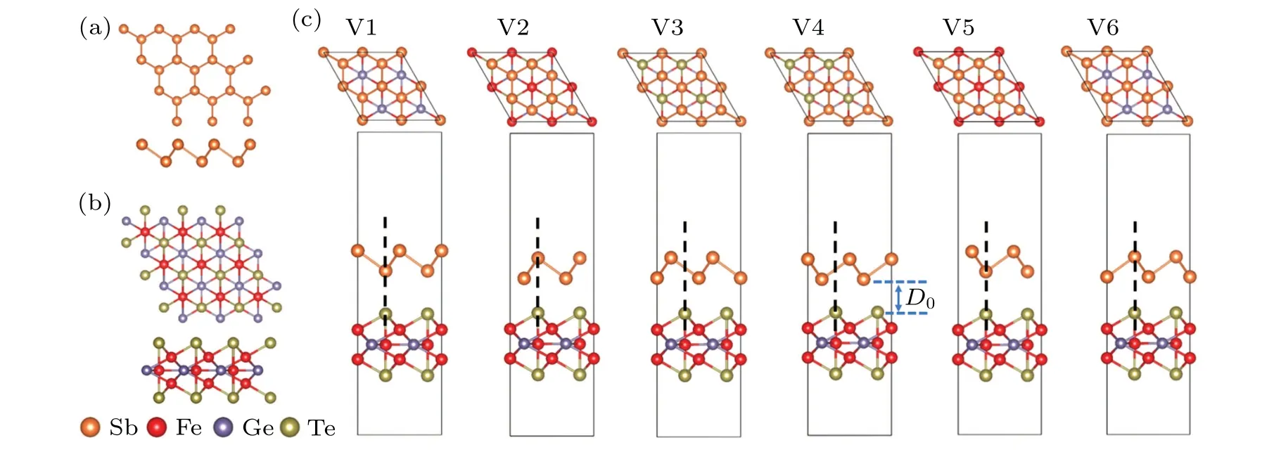
Fig.1. Structures of antimonene,Fe3GeTe2 monolayer and antimonene/Fe3GeTe2 vdW heterostructures. Top and side views of(a)antimonene and(b)Fe3GeTe2 monolayer. (c)The six different stacking configurations of the antimonene/Fe3GeTe2 vdW heterostructures.
We construct six different stacking configurations labeled by V1-V6,as shown in Fig.1(c). The dotted line indicates the perpendicular alignment. According to the atom alignment,six different configurations can be divided into three groups.V1 and V5 configurations belong to a group since the top Te atom of Fe3GeTe2is below the bottom Sb atom. The top Sb atom is just above the Te atom in V2 and V6 configurations.As for V3 and V4 configurations, the Te atom is right below the center of the hexagonal ring of antimonene.
The interlayer distance is defined as the perpendicular distance from the top Te atoms in the Fe3GeTe2monolayer to the bottom Sb atoms in the antimonene layer,which is labeled asD0in Fig. 1(c). The binding energyEbis calculated to compare the stability of the six different stacking configurations,which is defined as

whereEtis the total energy of the antimonene/Fe3GeTe2heterostructure,ESbis the energy of the freestanding antimonene,EFGTis the energy of the freestanding Fe3GeTe2monolayer,andSis the area of the unit cell. The interlayer distances and binding energies of six different stacking configurations are as shown in Table 1. Here, the lowerEbrepresents the more stable configuration.

Table 1. Optimized interlayer distances and binding energies of the heterostructures with different stacking configurations.
As shown in Table 1, the optimized interlayer distance of different configurations is from 2.78 °A to 3.59 °A, and the binding energy is in the range from-27.73 meV/°A2to-16.86 meV/°A2. It can be found that V4 configuration shows the smallest interlayer distance of 2.78 °A and the lowest binding energy of-27.73 meV/°A2, indicating that V4 is the most energetically favorable configuration. On the other hand, V1 and V5 have much higher binding energies than other configurations. It could be explained that the bottom Sb atom is just above the Te atom in V1 and V5 configurations,which will strengthen the repulsion between atoms and lead to higher binding energy.[40]Meanwhile, the binding energy is in the same magnitude of the other vdW heterostructure,such as Sb/InSe heterostructures(-23.86 meV/°A2),[41]which reveals that the antimonene and Fe3GeTe2monolayer interact with each other by van der Waals force. Since V4 is the most stable stacking configuration,it is used to further investigate the electronic structures and magnetic properties of the antimonene/Fe3GeTe2heterostructures,including the effect of external electric field and interlayer distance.
3.2. Electronic properties
The electronic properties of V4 configurations are investigated in this subsection. Figures 2(a)and 2(b)show the band structures of freestanding antimonene and the V4 configuration. The freestanding antimonene shows an indirect band gap of 1.13 eV(Fig.2(a)),comparable with the previous study.[42]As shown in Fig.2(b),the band gap of antimonene slightly decreases to 1.02 eV in the V4 configuration. The preservation of the original electronic states indicates that the main intrinsic properties of antimonene are preserved.
As shown in Figs.2(c)and 2(d),spin splitting appears at the CBM and VBM of the antimonene. Here, the energy difference between the spin-up and spin-down states at the CBM(VBM) is defined as ΔEc(ΔEv). The ΔEcis 246 meV, much larger than the ΔEv, which is only 24 meV. Besides, a certain degree of shift inkspace appears between the spin-up and spin-down bands of the CBM.
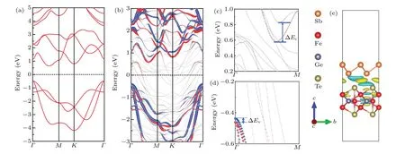
Fig. 2. Band structures and charge density difference. (a) Band structure of freestanding antimonene, and the Fermi level is set to zero. (b) Band structure of the V4 configuration. Red(blue)lines represent the spin-up(spin-down)band of antimonene in the heterostructure. (c)and(d)Zoom in the CBM and VBM of(b). (e)Charge density difference of the V4 configuration,the isosurface value is 0.0008 e/°A3. Yellow(blue)region represents net charge gain(loss).
The magnetic moment calculation results show that the bottom Sb atom close to the interface has a magnetic moment of-0.002μB, while the top Sb atom gains 0.001μB. The magnitude of the magnetic moment of Sb atoms is very small,which is mainly attributed to the weak interaction between antimonene and Fe3GeTe2.
The spin splitting shows that the magnetic proximity effect indeed exists in the antimonene/Fe3GeTe2vdW heterostructures. To explore the interaction in the antimonene/Fe3GeTe2heterostructures, the charge transfer has been calculated according to the following formula:

whereρSb/FGTis the total charge density of the antimonene/Fe3GeTe2heterostructure, and theρSbandρFGTrepresent the charge densities of the isolated antimonene and Fe3GeTe2monolayer,respectively. As shown in Fig.2(e),the charge transfer does exist between antimonene and Fe3GeTe2monolayer. Besides,the antimonene layer has a certain degree of charge depletion.
Through Bader charge analysis,[43,44]it is found that the antimonene layer loses 0.039eper unit cell. Therefore,a built-in electric field is generated. Similar charge transfer has been reported in other vdW heterostructures, such as arsenene/FeCl2heterostructure(0.03e).[45]

Fig.3. Spin-polarized total(a)and partial(b)-(e)DOS of the V4 configuration.
The total density of states(TDOS)and partial density of states(PDOS)of the antimonene/Fe3GeTe2heterostructure in V4 configuration are displayed in Fig. 3, demonstrating the states of different atoms.The hybridization of electronic states is also displayed. As shown in Figs. 3(a) and 3(c), the electronic states near the Fermi energy are mainly derived from the Fe d states. In addition, it can be drawn from Fig. 3(b)that antimonene still retains its semiconducting characteristic since there are no electronic states near Fermi level. Besides,there is a peak of Fe d states near 0.5 eV while there is no peak near-0.5 eV(as the red arrows marked in Fig.3),leading to a stronger hybridization between Fe 3d states and Sb 5p states at the CBM than the VBM. The stronger hybridization at the CBM can explain the larger spin splitting at the CBM.
3.3. Low-energy effective Hamiltonian
In order to better understand the spin splitting originated from the magnetic proximity effect, we focused on the band edges and proposed a low-energy effective Hamiltonian to capture the key features of the band structure.[46,47]
According to the band structure of freestanding antimonene obtained by the first-principles calculations(Fig. 2(a)), the low-energy physics near the band edges can be described by

wherem1andm2denote the effective masses of the two top valence bands near the band maximum at theΓpoint, andm3denotes the effective mass of the conduction band near the band minimum (Fig. 2(a)),kdenotes the momentum measured from theΓpoint,k0counts the distance between the VBM and the CBM,Δrepresents the width of the indirect bandgap, ands0is the two-by-two unit matrix. On the basis of this low-energy effective Hamiltonian, the influence of the ferromagnetic metal Fe3GeTe2to the antimonene can be captured by adding some appropriate terms. In accordance with the band structures for the whole heterostructure (Fig. 2(b)),we find that the key features of the influence can be described by the following modified low-energy Hamiltonian:


whereλ1,2,3denote the Zeeman splitting due to the magnetic proximity effect from the ferromagnetic metal Fe3GeTe2,szdenotes the third Pauli matrix in spin space,andδi=1,2,3,4denote the couplings between the CBM and the VBMs which originate from spin-conserving scatterings (by assuming thatszremains a good quantum number, and spin-flip scatterings are negligible). The couplings between the two groups of valence bands are negligible (H12=0). The reason is that they are originally degenerate at theΓpoint, suggesting that they originally belong to the same irreducible representation of the crystalline symmetry group. As theg-factor in real materials is band-dependent, soλ1,2,3are also band-dependent.The band-dependentλ1,2,3and the spin-conserving scatteringsδi=1,2,3,4provide a simple but physical picture to understand and explain the spin splitting and the spin-dependent bandedge momentum shift presented in Fig.2(b). According to the proposed low-energy Hamiltonian, the magnitude of the spin splitting energy at the CBM or VBM is mainly due to the parameterλ,which is set as relating to all the conditions,such as external electric field and interlayer distance. The spin splitting energy increases as the parameterλincreases.
3.4. Spin splitting under different modulations
Applying external electric field is an effective way to manipulate the properties of the vdW heterostructures.[48]To investigate the tunability of the spin splitting energy of CBM and VBM, a perpendicular external electric field is applied.The direction of the positive electric field is pointing from the Fe3GeTe2layer to the antimonene layer. As shown in Figs.4(a)-4(d),when the external electric field changes from-5 V/nm to 5 V/nm,ΔEcbecomes larger while ΔEvshows insignificant change. Figure 4(e)plots the spin splitting energies of the CBM (black line) and VBM (red line) in V4 configuration as a function of the external electric field. When the electric field changes from-5 V/nm to 5 V/nm, the ΔEcincreases from 227 to 262 meV monotonically. However, the ΔEvis much smaller than ΔEcand increases little as the electric field changes.
These results reveal that the application of external electric field can redistribute the electronic states of the heterostructure,leading to the modulation of the spin splitting energy in the antimonene/Fe3GeTe2heterostructure, mainly on CBM. Analogous to arsenene/FeCl2vdW heterostructures, it is reported that when the electric field changes from-5 V/nm to 4 V/nm,the spin splitting energy at the CBM increases from 98 meV to 166 meV.[45]
Simultaneously,the curve of the charge transfer with the external electric field is shown in Fig. 4(f), which reveals a negative linear relationship. This phenomenon indicates that the external electric field can promote or inhibit the charge transfer, leading to different interlayer interactions between antimonene and Fe3GeTe2monolayer.
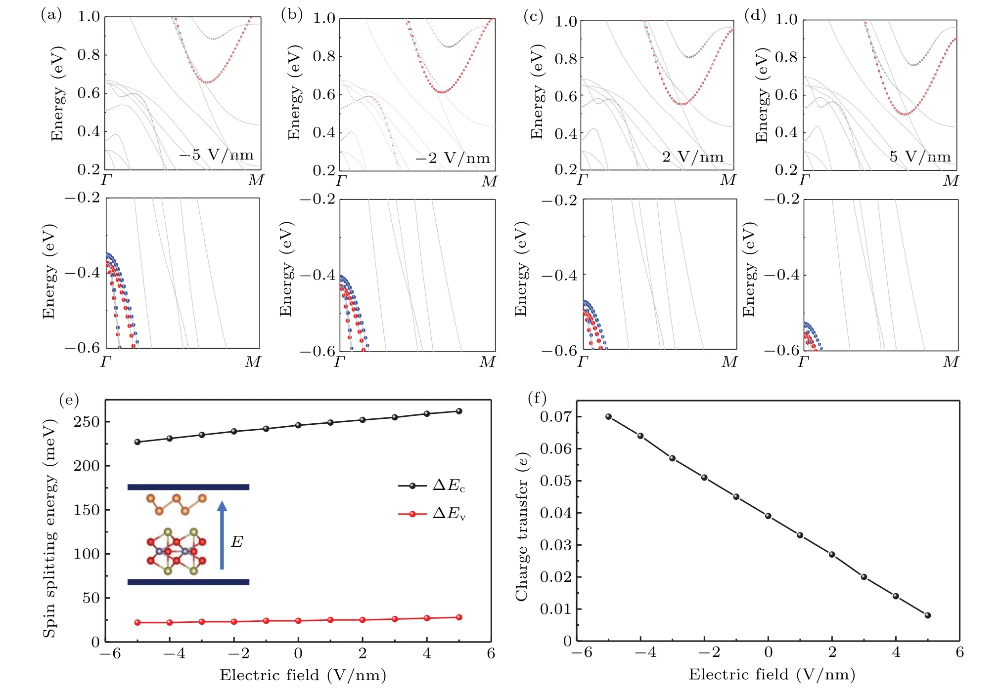
Fig. 4. Spin splitting and charge transfer under different external electric fields. Band structures at the CBM and VBM of V4 configuration under external electric fields of(a)-5 V/nm,(b)-2 V/nm,(c)2 V/nm,(d)5 V/nm. (e)The variation diagram of the spin splitting energy with different external electric fields. The inset shows the direction of the positive external electric field. (f)The variation diagram of charge transfer with different external electric fields.

Fig.5.Spin splitting under different interlayer distances and stacking configurations.Band structures at the CBM and VBM of V4 configuration under different interlayer distances of (a) 2.6 °A, (b) 3.0 °A, (c) 3.5 °A, (d) 4.0 °A. The variation diagram of the spin splitting energy with (e)different interlayer distances,(f)different stacking configurations.
The TDOS and PDOS of the V4 configuration under different external electric fields are plotted in Fig. B1. Though the distribution of the PDOS of-5 V/nm and 5 V/nm is similar,the hybridization of the peaks of Sb p states and the peaks of Fe d states are different.
The interlayer distance is also important to the electric structures of the vdW heterostructures. Changing the interlayer distance will bring a certain degree of vertical stress to the heterostructures, leading to the regulation of the band structures.[49]We studied the influence of different interlayer distances on the spin splitting by modulating the interlayer distance from 2.6 °A to 4.0 °A. As shown in Fig. 5(a), the spin splitting is clear in the interlayer distance of 2.6 °A.When the interlayer distance is 4.0 °A (Fig. 5(d)), the spin splitting at the VBM almost disappears. Meanwhile,when the interlayer distance increases, the degeneracy between the spin-up and spin-down bands is enhanced, as shown in Figs. 5(b)-5(d).The variation diagram of the spin splitting energy with different interlayer distances is plotted in Fig.5(e),which shows a trend that the spin splitting energy decreases monotonously as the distance increases. Furthermore,as shown in Fig.5(e),when the interlayer distance is less than the equilibrium interlayer distance(2.78 °A),the ΔEvdecreases more significantly than ΔEc. When the interlayer distance is 3.5 °A, the ΔEvis very close to zero. To further investigate the effect of different interlayer distances on electronic states of the heterostructures, we also calculated the TDOS and PDOS of V4 configuration at 2.6 °A and 3.5 °A,and found that the different magnitude of hybridization is in dependence of interlayer distance(Fig.B2). For instance,the magnitude of Sb p states near the VBM (-0.5 eV) at the interlayer distance of 2.6 °A is larger than that at 3.5 °A,leading to stronger hybridization and larger spin splitting energy.
Different stacking configurations of the heterostructures will induce different local environment,thus affecting the spin splitting.[50]The spin splitting under different stacking configurations is investigated by calculating the band structures of V1 to V6. As shown in Fig. C1, the band structures of different stacking configurations are quite similar, indicating that the intrinsic properties of each component are mainly preserved. However,the ΔEcand ΔEvare different,as displayed in Fig.5(f). As shown in Fig.5(f),the ΔEcand ΔEvof V1 and V5 configurations are similar,while V2 and V6 configurations possess similar spin splitting energy as well as V3 and V4.By comparing Fig.1(c), we can draw conclusion that similar configurations will lead to the same magnitude of interatomic interactions, resulting in similar spin splitting energy. On the one hand, the ΔEcand ΔEvof the V1 and V5 configurations are larger than those of other configurations, though the V1 and V5 configurations are not energetically favorable. On the other hand, V4 is the most stable structure among these six configurations and its ΔEcis slightly below V1 and V5.
Furthermore, since the magnetic moment mainly comes from the Fe atoms of Fe3GeTe2,the distance between the bottom Sb atom and top Fe atom may also affect the spin splitting.Thus, we also plot the nearest Sb-Fe distance under different configurations, as shown in Fig. D1. By comparing with Fig.5(f),it is found that spin splitting energy is not singly dependent on the nearest Sb-Fe distance.
From above discussion,it is found that the adjustment of spin splitting energy by applying an external electric field is mainly achieved by affecting the redistribution of electronic states. In addition,changing the interlayer distance and stacking configuration will affect the Sb-Fe distance and local electronic environment, which also has effect on the magnetic proximity effect.
4. Conclusion
In conclusion, the electric structures and magnetic properties of antimonene/Fe3GeTe2vdW heterostructure are investigated by the first-principles calculations. A low-energy effective Hamiltonian is proposed to depict the spin splitting at the CBM and VBM of the antimonene, which indicates that the spin splitting requires not only the effect of the magnetic field due to the Fe3GeTe2, but also the coupling between the conduction band and the valence band of the antimonene. The modulation of the spin splitting can be performed by different methods,such as applying external electric field,changing interlayer distance and changing stacking configuration. These modulations will change the hybridization of electronic states,the nearest Sb-Fe distance and local electronic environment,leading to the impact on magnetic proximity effect.
These results will help us to have a better understanding of the magnetic proximity effect in the vdW heterostructures as well as promote the application of the antimonene/Fe3GeTe2vdW heterostructures in the field of spintronic devices.
Acknowledgements
Project supported by the National Natural Science Foundation of China (Grant Nos. 11774434, 11974431, and 11832019). The computation part of the work was supported by National Supercomputer Center in Guangzhou.
Appendix A:Band structures of the V4 configuration without and with SOC

Fig.A1. Band structures of the V4 configuration without SOC(a)and with SOC(b).
Appendix B:TDOS and PDOS of V4 configuration under different external electric fields and interlayer distances

Fig.B1. TDOS and PDOS of V4 configuration under external field of(a)-5 V/nm and(b)5 V/nm.

Fig.B2. TDOS and PDOS of V4 configuration in interlayer distance of(a)2.6 °A and(b)3.5 °A.
Appendix C:Band structures of six different stacking configurations

Fig.C1. Band structures of different stacking configurations of(a)V1,(b)V2,(c)V3,(d)V4,(e)V5,(f)V6.
Appendix D: Nearest Sb-Fe distance under different configurations

Fig. D1. The distance between bottom Sb atom and the top Fe atom under six different configurations.
- Chinese Physics B的其它文章
- Measurements of the 107Ag neutron capture cross sections with pulse height weighting technique at the CSNS Back-n facility
- Measuring Loschmidt echo via Floquet engineering in superconducting circuits
- Electronic structure and spin-orbit coupling in ternary transition metal chalcogenides Cu2TlX2(X =Se,Te)
- Characterization of the N-polar GaN film grown on C-plane sapphire and misoriented C-plane sapphire substrates by MOCVD
- Review on typical applications and computational optimizations based on semiclassical methods in strong-field physics
- Quantum partial least squares regression algorithm for multiple correlation problem