
Dynamic vortex Mott transition in triangular superconducting arrays
2022-03-12 07:44ZiXiPei裴子璽WeiGuiGuo郭偉貴andXiangGangQiu邱祥岡
Chinese Physics B 2022年3期
Zi-Xi Pei(裴子璽) Wei-Gui Guo(郭偉貴) and Xiang-Gang Qiu(邱祥岡)
1Beijing National Laboratory for Condensed Matter Physics,Institute of Physics,Chinese Academy of Sciences,Beijing 100190,China
2School of Physical Sciences,University of Chinese Academy of Sciences,Beijing 100049,China
3Collaborative Innovation Center of Quantum Matter,Beijing 100084,China
Keywords: microfabrication,superconducting array,Mott transition
1. Introduction
Artificially fabricated superconducting systems have attracted much interest both in the study of vortex dynamics and applications because of its flexibility to tune the pinning and mutual interaction of vortices. One of such systems is the superconducting island arrays placed on normal metal films composing superconductor-normal-metalsuperconductor(SNS)structure.[1-5]With the proximity effect coupled superconducting island arrays, the superconducting vortices in this system[6]result in spatially arranged superconducting order parameters and move with a phase slip mechanism in the ‘eggcrate potential’ created by the underlying arrays. The pinning sites of the vortices are located between the islands where the potential minima exist.[7-9]At some special magnetic fields when the vortex lattice is commensurate with the arrays, the occupation of the pinning sites prevents the motion of the vortices and a vortex Mott insulating state emerges.[10]
In the previous works, the current-induced dynamic vortex Mott transition was firstly observed[3,5]in the square superconducting island arrays under a perpendicular magnetic field offflux quantum per unit cell. Different from the vortex depinning transition where the dips in the resistance versus magnetic field (R-f) curve disappear,[7,11]in the case of a dynamic vortex Mott transition a dip-to-peak reversal of the differential resistance versus magnetic field(dV/dI-f)curve near a rationalfwas observed while the dips in theR-fcurve existed during the transition. The transition is described by a scaling behavior resembling the electronic Mott transition and characterized by a single critical exponentε. The simulations of Josephson junction model with the same structure give the same critical exponent.[12,13]But in the simulation of a long-range Coulomb interaction between the vortices,[14]the scaling analysis gives a different critical exponent. It was concluded that the critical exponent is influenced by the interaction form between the vortices. As the potential landscape induced by the underlying arrays also influences the transition,it is interesting to investigate the transition in superconducting island arrays with different structures.
In this paper, current induced dynamic vortex Mott transition in triangular superconducting arrays has been studied. The dV/dI-fcurve shows that the dip-to-peak reversal emerges near the magnetic fields off=1 andf=1/2. Detailed measurements of dV/dI-fnear these two fields were performed to investigate the possible vortex Mott transition.It is found that the dV/dI-Icurves can be scaled as what is expected from a vortex Mott transition. The scaling behavior near the critical currents is the same as that in the square arrays[3]but with different critical exponentsε. For the case off=1/2,ε=0.45 and forf=1,ε=0.3, suggesting that in the current system, the vortex Mott transitions at integerfand fractionalfbelong to different universality classes.
2. Experiment
There are two different ways for the fabrication of the Nb island arrays. One is a bottom-up approach where the array is first exposed on a photoresist, followed by the deposition of Nb film on the exposed resist mask. Previous works[2,3,5,15]used this bottom-up microfabrication process because it is a convenient two-step approach.But such a bottom-up approach has disadvantages. For example, the resist residues at the exposed area may affect the Nb-Au interface and the shape of the array top can not be fully controlled. Besides,to avoid deposition on the resist sidewalls,a long distance between the source and the sample is necessary for the instrument. To avoid the above mentioned disadvantages,we developed a top-down approach to fabricate the superconducting island arrays. Before the microfabrication,the Au and Nb layers were deposited in a high vacuum chamber in which there were Au and Nb targets. As shown in Fig. 1(a), the standard top-down approach includes an electron beam lithograph (EBL) process for patterning the PMMA resist arrays as a mask on the top of the Nb film. Then a reactive ion etching(RIE)process is followed to remove the uncovered Nb film. After dissolving the resist in acetone,the sample was obtained. The EBL exposing area of the PMMA resist in this method is shown in Fig.1(b). As the exposed area has an irregular shape,the residual resist arrays after the EBL process can hardly keep a circular shape because of the optical proximity effect. Here we developed a new method on the basis of the standard top-down approach.As shown in Fig.1(c),the EBL process was used to create the resist mask not for etching but for Al deposition. Such that the exposed area was circular arrays, as shown in Fig. 1(d). By doing so, the influence of the optical proximity effect for the island shape can be avoided. The Al island arrays were fabricated after the electron beam deposition(EBD)and a PMMA lift-off process, which was then served as a hard mask. We chose Al as the hard mask because in the RIE process of Nb the consumption of Al mask can be ignored and it can be easily removed. Then the Nb film was etched with the mixture of Ar and SF6as working gas. As the etching speed of Au film is far lower than that of Nb with the working gas,it is easy to control the etching time so that the uncovered Nb layer was completely etched without damaging the Au layer. Finally the Al mask was washed out with weak alkaline solution. With this top-down microfabrication approach,we successfully prepared high quality samples with cylindric shaped island arrays.

Fig. 1. (a) The standard top-down approach for microfabrication. (b) The exposing area of patterning the photoresist as a mask for etching. (c) The improved microfabrication process for a better island shape. (d)The exposing area of patterning the photoresist as a mask for deposition.

Fig.2. (a)Scanning electron microscopy image of the triangular Nb island arrays on Au film,the insert is the bridge for transport measurements.(b)A magnified scanning electron microscopy image of the same sample. (c)Atom force microscopy image of the same sample. (d)The resistance versus temperature curve near the critical temperature.
The 90 nm Nb and 50 nm Au layers were deposited on 1×1 cm2Si/SiO2substrate with magnetic sputtering process.The UV exposure was used to pattern a resist mask then the micro-bridge for transport measurements was created by the RIE processes. The central area of the bridge is 60×60 μm2with four terminals as electrods.Then a EBL process was used to pattern the 90×65 μm2resist mask covering the bridge center. After that, the hard mask was created by Al deposition and the PMMA lift-off process. Then the sample was etched by a RIE process to remove the part of Nb layer uncovered by the Al mask. After the etching,the hard mask can be washed out by AZ 300MIF solution. As shown in the insert of Fig.2(a),the patterned area of 90×65 μm2was at the center of the bridge, covering an area of 60×60 μm2. As shown in Figs. 2(a)-2(c), each Nb island has a cylindrical shape, with a diameterd= 180 nm, a heighth= 90 nm, and a perioda=270 nm.
All the transport measurements were carried out in the Quantum Design PPMS-9. The applied DC current was introduced by the Keithley Model 6221 DC current source and the DC voltage was measured by the Keithley Model 2182 nanovoltmeter. The applied AC current was introduced by the Lakeshore Model 370 AC resistance bridge, which was also used to measure the differential resistance(dV/dI). The critical temperature of the sample, determined as the 50%of the nomal state (9 K) resistance, was about 7.9 K as shown in Fig.2(d). The high critical temperature indicates that the coupling energyEJbetween the superconducting arrays is strong enough to obtain a high vortex pinning potential for forming the vortex Mott insulator state.[2,16]
3. Results and discussion


Fig. 3.(a) Resistance (R) versus magnetic field (f) curve with different applied currents, minima were found at f =0,1/4,1/3,3/8,1/2,5/8,2/3,3/4,1. (b) Differential resistance (dV/dI)versus magnetic field (f) with different applied currents, minima were found at f =0,1/4,1/3,3/8,1/2,5/8,2/3,3/4,1 with low applied current,dip-to-peak reversals occur at f = 1/2 and f = 1 with the increasing of the applied current. The R-f and dV/dI-f curves were measured simultaneously at 2 K with different currents.


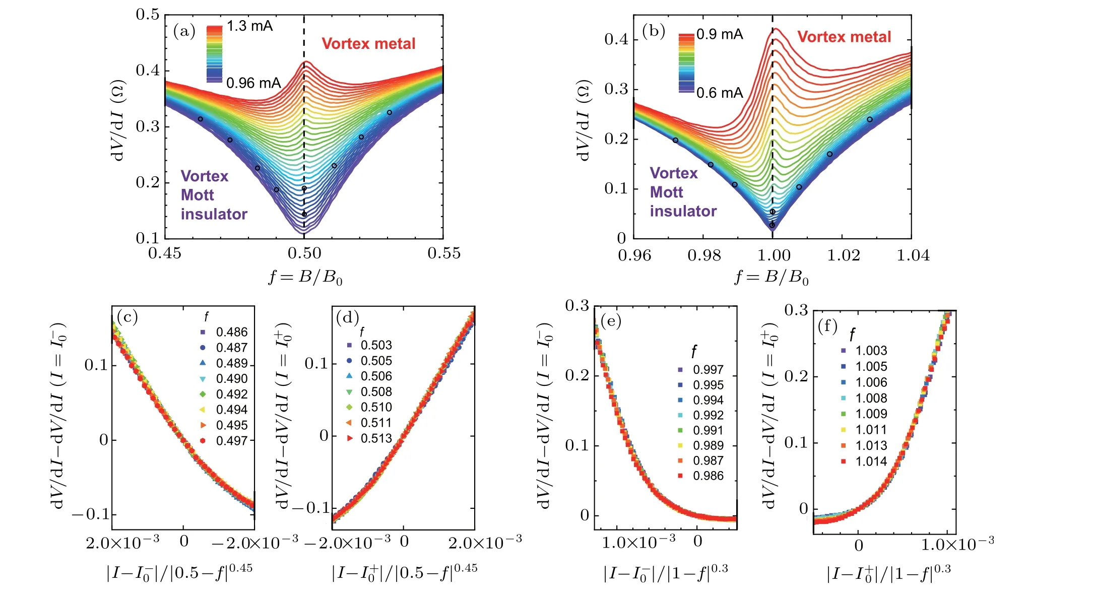
Fig.4. (a)The dV/dI versus f curve measured near f =1/2 with applied current from 0.96 mA to 1.3 mA.(b) dV/dI versus f curves measured near f =1 with applied current from 0.6 mA to 0.9 mA.The figure contains the curves measured with different applied currents of 10 μA interval.The critical currents I±0 were determined where the dips at f =1/2 and f =1 disappeared. There are slight differences between critical currents below and above the two fields, written as I-0 and I+0 . For f =1/2 case, I-0 =1.02 mA and I+0 =1.07 mA. For f =1 case, I-0 =0.65 mA and I+0 =0.68 mA.(c)and(d)Scaling of dV/dI-I curve measured at different fields near f =1/2. The critical exponent ε=0.45. (e)and(f)Scaling of dV/dI-I curves measured at different fields near f =1. The critical exponent ε =0.3.
4. Conclusion
We have developed a top-down micro-fabrication process to fabricate superconducting Nb island arrays on Au film by employing an Al hard mask. High quality samples with triangular Nb island arrays on Au film have been obtained. The relatively high superconducting critical temperature indicates a strong coupling between the superconducting islands. Commensurate fields in the field dependent resistance have been observed in integer and fractionf, which is consistent with the calculated results. A dip-to-peak reversal in the dV/dI-fcurve has been found near the fields off=1/2 andf=1.The scaling analysis reveals that the dip-to-peak reversals in the two fields are associated with the dynamic vortex Mott transition,the different critical exponents at these two fields suggest that the transitions belong to different universality classes.
Acknowledgments
X.G.Q.acknowledges the support from the National Natural Science Foundation of China (Grant Nos. 11974412 and 11774400) and the National Key R&D Program of China(Grant Nos.2017YFA0302903 and 2018YFA0305703).

- Chinese Physics B的其它文章
- Measurements of the 107Ag neutron capture cross sections with pulse height weighting technique at the CSNS Back-n facility
- Measuring Loschmidt echo via Floquet engineering in superconducting circuits
- Electronic structure and spin-orbit coupling in ternary transition metal chalcogenides Cu2TlX2(X =Se,Te)
- Characterization of the N-polar GaN film grown on C-plane sapphire and misoriented C-plane sapphire substrates by MOCVD
- Review on typical applications and computational optimizations based on semiclassical methods in strong-field physics
- Quantum partial least squares regression algorithm for multiple correlation problem