
Facile sensitizing of PbSe film for near-infrared photodetector by microwave plasma processing
2022-03-12 07:44KangyiZhao趙康伊ShuanglongFeng馮雙龍ChanYang楊嬋
Chinese Physics B 2022年3期
關鍵詞:雙龍
Kangyi Zhao(趙康伊) Shuanglong Feng(馮雙龍) Chan Yang(楊嬋)
Jun Shen(申鈞)2, and Yongqi Fu(付永啟)1,?
1School of Physics,University of Electronic Science and Technology of China,Chengdu 610054,China
2Chongqing Institute of Green and Intelligent Technology,Chinese Academy of Sciences,Chongqing 400714,China
Keywords: PbSe film,infrared photodetector,plasma processing
1. Introduction
PbSe is a typical narrow bandgap semiconductor material with full application in infrared detectors.[1-5]For photodetectors, high quality PbSe film has been successfully fabricated by chemical bath deposition,[6]electrochemical deposition,[7]thermal evaporation,[8]and molecular beam epitaxy method[9]during the past two decades. When making devices from materials, it is often necessary to sensitize PbSe under an oxygen/halogen atmosphere to improve the stability of devices and reduce noise, which is a critical process that determines the performance of photodetectors.[10-15]For a long time,scientists worldwide have researched the sensitization method and sensitization mechanism of PbSe based devices.[16-19]For example,Humphrey and Scanlon reported that the p-n type of PbSe film can be converted by doping the halogen group during thermal sensitization.[20]Zhaoet al.introduced a charge separation junction model to further explain the sensitization mechanism of the PbSe photodetector.[21]However,studies on plasma as the sensitization method of PbSe thin film are relatively few.
In this work, the higher-reaction active ground states of microwave plasma were utilized to sensitize the PbSe thin film.[22-26]The morphology, crystal structure, and elemental composition of the sample before and after plasma processing were investigated in detail. By comparing the performance of photodetectors,the detectivity(D*)of a plasma-sensitizing PbSe-based device is found to be 17.5 times better than that of the raw materials. Finally,the mechanism of plasma sensitization is also discussed based on the Hall effect test.
2. Experimental details
2.1. Materials synthesis and sensitizing
The 500 nm PbSe thin film was deposited on Si/SiO2substrates by a thermal evaporation method. Before deposition,the Si/SiO2substrates were ultrasonically cleaned with acetone, deionized water, and ethanol in sequence. High-purity PbSe powder(99.99%)was loaded in a graphite crucible with a crucible/substrate distance of about 26 cm in the vacuum chamber. The substrate temperature was set to 200°C and the vacuum pressure was about 5.5×10⁻⁴Pa. Subsequently,the PbSe film was processed in a homemade microwave plasma chemical vapor deposition (MPCVD) process consisting of a domestic microwave oven (with the power set at 700 W,2.45 GHz), a gas supply system, a quartz tube (25 mm outer diameter)and a vacuum pump. Gaseous Ar2(70 sccm)flowed into the quartz tube accompanied by continuous pumping and maintained at a base pressure of about 10-1Pa. Then, Ar plasma with bright purple color was generated when the microwave was turned on.Finally,the microwave oven/gas valve was closed and the treated sample was taken out.
2.2. Material characterization
The crystal structure of the film was identified by an x-ray diffractometer (XRD, Bruker D8-Focus). The surface morphology and elemental composition of the film were characterized by a scanning electron microscope(SEM,Shimadzu, SSX-550) equipped with energy-dispersive spectroscopy(EDS).The optical properties(absorption and reflectivity) of the film were recorded using a near-infrared (NIR)spectrophotometer(Gangdong,S410).
2.3. Photoresponse measurement
Both theI-Vcharacteristics and photoresponses of the fabricated devices were recorded by a Keithley 4200 source meter at room temperature. Photoresponse measurement was carried out at a laser wavelength of 1550 nm, and the current was measured while the illumination was modulated between on and off with a shutter controlled by a square wave signal. To further evaluate the photodetector performance of the PbSe film via Ar plasma by MPCVD equipment,a PbSebased photoconductor was fabricated on a SiO2/Si substrate(0.4 cm×0.2 cm). In this structure,photolithography patterns were formed by photolithography (shadow-mask-used). An ohmic contact with Cr/Au(3 nm/50 nm)electrodes was realized by e-beam deposition and standard lift-off process; the effective photoactive area of PbSe was 0.2 cm×0.2 cm.
3. Results and discussion
Figure 1(a) shows the XRD patterns of the thermally evaporated PbSe films as a function of plasma handling time.The diffraction peaks correspond to the (110), (111), (200),(012), (220), (311), (400), and (204) planes, which can be indexed to the cubic PbSe phase in good agreement with the JCPDS card 06-0354. Although some oxide diffraction peaks appear in the diffraction pattern,the PbSe diffraction peaks are still dominant, such as the(200)-serial diffraction peak. This indicates that the interior of the grain is still PbSe, and only the surface layer of the PbSe grain is partially oxidized. The predominant(200)-serial diffraction peaks are observed for all samples,the intensities of which are enhanced with increasing microwave time. This behavior should be attributed to the improvement in the corresponding diffraction orientations. The full width at half maximum (FWHM, denoted asβ) of the(200)peak,which has been calibrated by deducting the instrumental broadening,decreases with increasing microwave time until reaching a minimum value at 6 min, and then increases with a continuous increase in plasma handling time. This reveals that the crystallinity of the films is improved with increasing microwave time,reaching a maximum at 6 min. Subsequently,the absorptivity of PbSe films with different plasma handling times is also investigated, as shown in Fig. 1(b). It indicates that the infrared absorptivity did not change significantly under different microwave treatment times, fluctuating within 62%-72%,with the lowest absorptivity at 8 min under microwave treatment. Finally, the atomic ratios of Pb, Se, O,and Si are obtained by EDS, as shown in Fig. 1(c). During the plasma treatment (0-8 min), the atomic ratio of Pb and Se is approximately 1:1; the proportion of O atom decreases slightly compared with no plasma treatment, but the O atom proportion changes little as the subsequent plasma processing time increases from 2 min to 8 min as shown in Fig. 1(d).It is reasonable that plasma treatment causes a sintering phenomenon in the PbSe thin film and improves the degree of crystallization.

Fig.1.(a)XRD patterns of PbSe film with different microwave processing times;(b)optical absorption spectrum of the PbSe film under different microwave processing times;(c)atomic ratios of Pb,Se,O,and Si as a function of time plotted in the histogram;(d)content curve of O element in the samples under different handling times.
The SEM images of the PbSe film with different plasma handling times are illustrated in Fig.2. For the PbSe film with plasma handling timet=0 min in Fig.2(a),the PbSe thin film is composed of particles agglomerated by nanocrystals, and the film layer is continuous with a dense structure. With the treatment of Ar plasma for 2 min, the PbSe film is no longer granular and presents features of high crystal quality, dense structure,and excellent uniformity,as shown in Fig.2(b). The crystallinity of the PbSe thin film continues to increase with increasing microwave plasma action time until some holes appear on the thin film under the etching process of Ar ions.With the increase in etching time,an increasing number of holes are found in the film,as shown in Figs.2(c)-2(e).
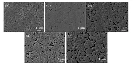
Fig.2. SEM image of treated PbSe film: (a)0 min;(b)2 min;(c)4 min;(d)6 min;(e)8 min.
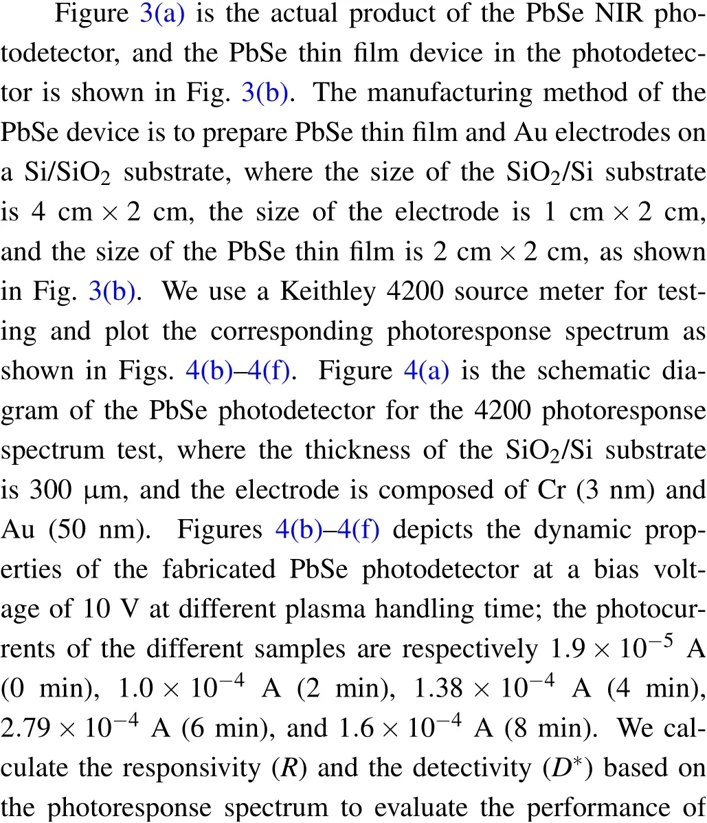


Fig. 3. (a) PbSe photodetector with a microwave time of 6 min; (b) PbSe device with dimensions.


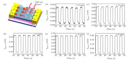
Fig.4. (a)Schematic of the PbSe photodetector;photoresponse spectra under the illumination of λ =1550 nm at different microwave processing times(bias voltage is 10 V):(b)0 min;(c)2 min;(d)4 min;(e)6 min;(f)8 min.

Fig.5. Response time diagram at different microwave processing times: (a)2 min;(b)4 min;(c)6 min;(d)8 min.

Table 1. Responsivity(R),detectivity(D*)and response time data list at different plasma time.

Fig.6.(a)The I-V curve of the PbSe photodetector with microwave time t=6 min(dark current/1550 nm);(b)voltage noise spectral density measured at plasma time t=6 min.
We analyzed the performance of the PbSe photodetector under the optimal sensitization conditiont=6 min. We obtained the photoresponse spectra of the PbSe films as a function of voltage and the photocurrent of the PbSe films as a function of optical power, as shown in Figs. 7(a) and 7(b).As can be seen in Fig. 7(a), the microwave processing time is 6 min and the incident light wavelength is 1550 nm. When the power of the light source is stable, the device photocurrent increases with an increase in the bias voltage. When the power of the incident light source is constant, the number of carriers generated per unit area of the film surface is constant.In this case,the greater the bias voltage,the more carriers can be effectively separated by the device, so the photocurrent of the device is larger.When the bias voltage of the test system is 10 V,Y=0.06163X+2.3985×10⁻⁴.Because the system bias voltage is constant, increasing the power of the incident light source increases the number of photogenerated carriers generated per unit area of the film and the device generates a larger photocurrent. The PbSe infrared photodetector experimental result is consistent with the theoretical analysis,indicating that the device meets expectations.

Fig.7. (a)Photoresponse spectra of PbSe film as a function of voltage under the illumination of λ =1550 nm(Plight=5×10⁻⁴ W);(b)photocurrent of PbSe film as a function of optical power(U =10 V).
A Hall effect tester (L79/HCS) is used to test the Hall coefficient,carrier concentration,migration rate,and conductivity to understand the change in the plasma-processed photodetector. The results are shown in Table 2. The positive Hall coefficient indicates that the PbSe film before and after plasma processing is p-type. As the action time of Ar plasma increases,the conductivity and the migration rate of the PbSe film initially gradually increase and then decrease,reaching a maximum when the plasma treatment time is 6 min. At this time,the conductivity of the PbSe thin film is 0.06872 Ω·cm,and the migration rate of the PbSe film is 11.553 cm2/(V·s).The photoelectric performance is best when the responsivity(R) and detectivity (D*) of the PbSe film are at a maximum.In summary,the PbSe layer as a volatile precursor participates in a chemical reaction during the MPCVD process;Ar plasma diffuses from the surface of the PbSe thin film to the inside and reacts with the PbSe film,resulting in a secondary deposition on the PbSe layer itself,which improves the photoelectric performance of the PbSe film significantly.
4. Conclusion
In summary, PbSe thin film was fabricated by a thermal evaporation method, and Ar plasma realized the sensitization of a PbSe photodetector. The responsivity and detectivity of the PbSe photoconductor can be improved by an order of magnitude after quick plasma sensitization. The detectivity of a plasma sensitizing PbSe based devices is 17.5 times better than that of the raw materials. The response time reaches the magnitude of microseconds,providing a potential method of fabricating high-performance PbSe-based optoelectronic detectors.
Acknowledgments
Project supported by the National Natural Science Foundation of China (Grant Nos. 61605207, 61704172, and 61705229), the Key Research and Development Plan of the Ministry of Science and Technology of China (Grant No. 2017YFE0131900), the Western Light Program of the Chinese Academy of Sciences, and Youth Innovation Promotion Association of Chinese Academy of Sciences (Grant No.2018416).
猜你喜歡
Chinese Physics B(2022年4期)2022-04-12
現代裝飾(2021年6期)2021-12-31
中國土壤與肥料(2020年6期)2021-01-18
越玩越野(2015年2期)2015-08-29
中國新時代 (2009年3期)2009-11-26
環球時報(2009-08-04)2009-08-04
環球時報(2009-05-07)2009-05-07
環球時報(2009-01-22)2009-01-22
環球時報(2009-01-06)2009-01-06

- Chinese Physics B的其它文章
- Measurements of the 107Ag neutron capture cross sections with pulse height weighting technique at the CSNS Back-n facility
- Measuring Loschmidt echo via Floquet engineering in superconducting circuits
- Electronic structure and spin-orbit coupling in ternary transition metal chalcogenides Cu2TlX2(X =Se,Te)
- Characterization of the N-polar GaN film grown on C-plane sapphire and misoriented C-plane sapphire substrates by MOCVD
- Review on typical applications and computational optimizations based on semiclassical methods in strong-field physics
- Quantum partial least squares regression algorithm for multiple correlation problem