
Interfacial molecular screening of polyimide dielectric towards high-performance organic field-effect transistors
2024-04-05 02:28YngsuangZengHucaoTngJangFeJaoJeYongLeGuoengTanJnsunYundongXuanLqangDeyangWenpngHu
Chinese Chemical Letters 2024年2期
Yngsuang Zeng ,Hucao L ,Tng Jang ,Fe Jao ,Je L ,Yong Le ,Guoeng Tan,Jnsun B,Yundong Xuan,Lqang L,*,Deyang J,*,Wenpng Hu
a Department of Chemistry,Tianjin Key Laboratory of Molecular Optoelectronic Sciences,Institute of Molecular Aggregation Science,Tianjin University,Tianjin 300072,China
b GPL Photonics Laboratory,State Key Laboratory of Applied Optics,Changchun Institute of Optics,Fine Mechanics and Physics,Chinese Academy of Sciences,Changchun 130033,China
c Haihe Laboratory of Sustainable Chemical Transformations,Tianjin 300192,China
d Department of Chemistry,Tianjin Key Laboratory of Molecular Optoelectronic Sciences,School of Science,Collaborative Innovation Center of Chemical Science and Engineering,Tianjin University,Tianjin 300072,China
e Joint School of National University of Singapore and Tianjin University,Fuzhou 350207,China
f Fachgebiet Angewandte Nanophysik,Institut für Physik & IMN MacroNano,Technische Universit?t Ilmenau,Ilmenau 98693,Germany
g State Key Laboratory of Chemical Resource Engineering,Beijing University of Chemical Technology,Beijing 100029,China
h Institute of Microelectronics,Chinese Academy of Sciences,Beijing 100029,China
i University of Chinese Academy of Sciences,Beijing 100101,China
Keywords: Interfacial molecular screening Polyimide dielectrics Organic semiconductors Interface engineering Thin-film transistors
ABSTRACT The compatibility of the gate dielectrics with semiconductors is vital for constructing efficient conducting channel for high charge transport.However,it is still a highly challenging mission to clearly clarify the relationship between the dielectric layers and the chemical structure of semiconductors,especially vacuum-deposited small molecules.Here,interfacial molecular screening of polyimide (Kapton) dielectric in organic field-effect transistors (OFETs) is comprehensively studied.It is found that the semiconducting small molecules with alkyl side chains prefer to form a high-quality charge transport layer on polyimide (PI) dielectrics compared with the molecules without alkyl side chains.On this basis,the fabricated transistors could reach the mobility of 1.2 cm2 V-1 s-1 the molecule with alkyl side chains on bare PI dielectric.What is more,the compatible semiconductor and dielectric would further produce a low activation energy (EA) of 3.01 meV towards efficient charge transport even at low temperature (e.g.,100 K,0.9 cm2 V-1 s-1).Our research provides a guiding scheme for the construction of high-performance thin-film field-effect transistors based on PI dielectric layer at room and low temperatures.
Interfaces in organic electronics play a pivotal role in modulating the device performance,which has been fully verified in the past three decades [1-6].Thereinto,the introduction of polymer dielectrics into organic devices offers more possibility of tuning the device interface and then optimizing the device performance due to designable monomeric structures and adjustable surface characteristics [7].Despite remarkable progress in achieving effi-cient charge transport has been made on polymer dielectric,the reported studies mainly discussed the performance of a certain organic semiconductor (OSC) on either dielectric layer with variable interfaces [8-11],or a fixed dielectric layer [12-14],resulting in the unclear relationship between the dielectrics and chemical structures of semiconductors.Therefore,to further investigate the selectivity of specific dielectric layer to semiconducting molecules is necessary,which would help more effectively screen the dielectric and semiconductor materials with better compatibility for highperformance organic devices.As one of the earliest polymer dielectrics used in organic field-effect transistors,polyimide (PI) with satisfactory advantages of high/low temperature stability,solvent resistance and excellent stability [15-18],has exhibited promising applications in today’s microelectronics [6,7].However,it is worth noting that most of the devices based on bare PI dielectrics show lower mobility than thin-film amorphous silicon devices of 0.5-1 cm2V-1s-1[17,19-21],only a few cases of modified PI could obtain the mobility exceeding 1 cm2V-1s-1(Fig.S1 in Supporting information) [22-25].On this basis,how to correctly evaluate the compatibility of bare PI with semiconductors and improve the device performance is becoming the key point.
Here,three groups of organic small molecules with and without alkyl chains are used as active layers to vapor-deposit onto bare PI for constructing thin-film devices.It was found that bare PI had a molecule-selective interface,which preferred to select the semiconducting molecules with alkyl chains forming efficient conducting channel for high charge transport possibly due to the strong intermolecular interactions at the interface.As a result,the mobility of devices with bare PI and alkyl-chains-based molecular structure could reach 1.2 cm2V-1s-1,which is one of the highest mobilities of thin film transistors based on bare PI dielectric reported in the existing literature (Fig.S1).Simultaneously,a low activation energy (EA) of 3.01 meV was achieved,demonstrating a low degree of disorder present in the films of molecules with alkyl side chains on the surface of the PI dielectric.In addition,the better compatibility of bare PI with semiconductors could also promote the device with efficient charge transport at low temperature(e.g.,100 K) and obtain a relatively stable device at low temperature.The selectivity relationship between PI and semiconductors provides an instructive strategy for the application of PI dielectric in high-performance organic thin-film transistors at room and low temperatures.
As shown in Fig.1a,the OFET device with bottom-gate topcontact (BGTC) structure was used to study the molecule-screening interface of bare PI dielectric layer.Here,three groups of representative organic small molecules with and without alkyl chains were selected (Fig.1a).Vacuum-deposited method is an effective approach to investigate the interface effect of the device due to the sensitivity of molecular growth to the device interface [5,13].First of all,the surface morphology of the semiconductor layer on the PI dielectric layer was analyzed by atomic force microscopy(AFM).As shown in Fig.S2 (Supporting information),the roughness of interface based on organic semiconductors without alkyl side chains (e.g.,DPA,DNTT and 2,6-DNA) was larger than those with alkyl side chains (e.g.,C6DPA,C10DNTT,C10-2,6-DNA).Obviously,more ordered morphology of thin films was observed from deposited molecules with alkyl side chains on PI (Fig.S3 in Supporting information).As a result,it is clearly shown in Fig.1b that the devices using semiconductors without alkyl side chains exhibited suppressed mobility of~10-3cm2V-1s-1due to the weak interaction between the PI strands and the semiconductors [26],but those semiconductors with alkyl side chains could construct efficient conducting channel on bare PI for up to three orders of magnitude higher performance possibly due to the strong interaction between the PI strands and the semiconductors.The representative transfer and output curves based on different semiconductors were shown in Figs.1c-e and Fig.S4 (Supporting information),respectively.What is more,from the analysis of the transfer curve (Figs.1c-e),not only the output current but also the on/off ratio has been improved by several orders of magnitude using organic semiconductors with alkyl side chains.In order to verify the uniqueness of molecule-screening PI interface,bi-polymer dielectrics on the basis of polystyrene (PS) and polyphenylene ether(PPO) as the buffer layers to modify the PI were used to prepare the OFET device (Fig.2a).It was obvious that the introduction of PPO and PS buffer layers could enhance the device mobility based on some small molecules,but the existence of PPO and PS would change the screening characteristics of molecules at the interface(Figs.2b and c,Figs.S5 and S6 in Supporting information).These results could further suggest that the apparent difference in the device mobility based on bare PI was attributable to the selective interaction between PI and semiconductor molecules.
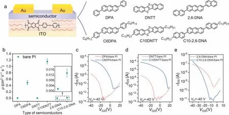
Fig.1.(a) Schematic diagram of organic thin-film FETs with BGTC and different semiconductor molecular structures.(b) Mobility distribution of transistors based on different semiconductors and bare PI.The typical transfer curves of transistors based on bare PI dielectrics using (c) DPA and C6DPA,(d) DNTT and C10DNTT,(e) 2,6-DNA and C10-2,6-DNA as active layers.

Fig.2.(a) Schematic diagram of the device with buffer layers.Mobility distribution of transistors based on different semiconductors and (b) PPO/PI and (c) PS/PI.(d)Schematic diagram of organic single crystal transistor devices constructed by transferring pre-grown organic single crystals and gold electrodes,respectively.Transfer curves of devices with pre-grown (e) DPA,(f) C6DPA and (g) DNTT single crystals transferred onto PI dielectric,respectively.Inset: optical images of the fabricated single crystal OFETs.Scale bar: 90 μm.
Subsequently,we transferred organic single crystals with order molecular stacking on bare PI surface to further investigate its interface effect.The details about the fabrication of single crystal are shown in the experimental section in Supporting information [27].Here,DPA,C6DPA and DNTT were chosen as examples to prepare the single-crystal OFETs (Fig.2d).In this kind of device,the source/drain gold electrodes were constructed by transferring the gold film by mechanical probes [28].The typical transfer and output curves of single-crystal devices were shown in Figs.2e and f,and Figs.S7a and b (Supporting information),respectively,compared to C6DPA device (μ=1.06 cm2V-1s-1),DPA device(μ=4.08 cm2V-1s-1) exhibited even better charge transport performance.In addition,DNTT single crystal devices also had higher mobility (μ=1.71 cm2V-1s-1) compared with thin-film devices(Fig.2g and Fig.S7c in Supporting information).These results showed that the PI interface could also produce efficient charge transport based on organic semiconductors with order molecular stacking (e.g.,single crystal),but this interface had an influence on the directly vacuum-deposited growth of molecules with different chemical structures.
TheEAcalculated from temperature-variable experiments is an important factor to assess the degree of disorder presented at the interface [29,30].Based on the low-temperature stability of PI dielectric layer [17,29],the devices using different semiconductors were carried out temperature-variable electrical tests (Fig.S8 in Supporting information).The temperature-dependent mobility curves showed the typical hopping mode in all kinds of devices because of the decreasing values of mobility with the decrease of the temperatures (Fig.S9 in Supporting information).According to theμ=μ0·exp(-EA/kBT) [29],whereμis carrier mobility at different temperatures,EAis activation energy,kBis Boltzmann constant,andTis thermodynamic temperature.The calculatedEAconsistently indicated that the values of devices using organic semiconductors with alkyl side chains (C6DPA,11.20 meV,Fig.3a;C10DNTT,3.01 meV,Fig.3b),were significantly lower than that using organic semiconductors without alkyl side chains (DPA,24.15 meV,Fig.S10 in Supporting information;DNTT,40.4 meV[31]).The calculated value ofEAcould clearly indicate that the organic semiconductors with alkyl chains preferred to form highquality packing of semiconductor molecules and a lower degree of interface energy disorder at the interface of PI.It was worth noting that our fabricated devices exhibited one of the lowest values ofEA(3.01 meV) compared with the previous reports [11,30,32-39] as shown in Table S1 (Supporting information),which demonstrated that our devices could still maintain efficient charge transfer,even at low temperatures.For example,the device based on C10DNTT on bare PI dielectric showed the mobility of 1.2 cm2V-1s-1at 300 K,and then,the decrease of temperatures only reduced the mobility by 25%,maintaining 0.9 cm2V-1s-1at 100 K (Fig.S9b in Supporting information).More excitingly,the device using C10DNTT and PS/PI dielectric could still maintain the mobility about 1.0 cm2V-1s-1at 100 K (Fig.S11 in Supporting information).This efficient charge transport performance at low temperature indicated the excellent compatibility of the low temperature resistance of PI and high-quality stacking of C10DNTT for further low-temperature applications.In addition,we also found that PI-based devices all showed atmospheric stability after one year(Fig.4a).Moreover,the efficient charge transport would contribute to the high-performance optical figures of merit in organic phototransistors (OPTs) [35,40].We fabricated the thin film OPTs using bare PI dielectric and the semiconductors with alkyl side chains and high mobility (e.g.,C6DPA,C10DNTT).The best value of calculated optical figures of merit,including photosensitivity (P),photoresponsivity (R) and detectivity (D*),were plotted in Figs.4b and c.It was clearly seen that the OPTs using bare PI dielectric and the semiconductors with alkyl side chains showed higher performance than that with bare PI dielectric and alkyl-side-chains-free semiconductors [31].Furthermore,the switching performance based on semiconductors with alkyl side chains was also higher than that devices using semiconductors without alkyl side chains,as shown in Figs.S12-S14 (Supporting information),respectively.
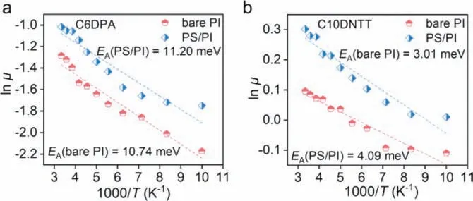
Fig.3.Fitting results of low temperature mobility and temperature according to Arrhenius formula.(a) C6DPA/bare PI and C6DPA/PS/PI,(b) C10DNTT/bare PI and C10DNTT/PS/PI.
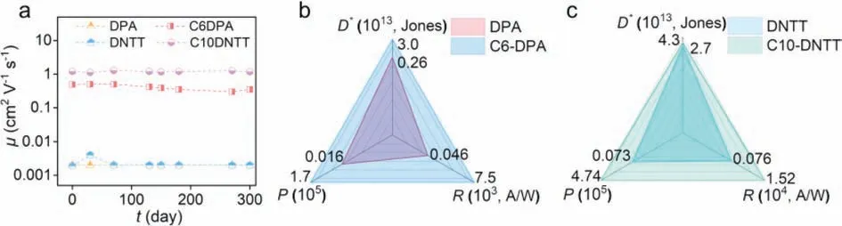
Fig.4.(a) The stability performance of device mobility based on bare PI and different semiconductors.The best value of photosensitivity (P),photoresponsivity (R) and detectivity (D*) using (b) DPA and C6DPA;(c) DNTT and C10DNTT.
Although the potential application of polyimide dielectric in organic field-effect transistors has been verified,the device performance based on polyimide dielectric still lagged behind other dielectric materials.In this work,we have found there is interfacial molecular screening of polyimide dielectric on semiconductors in organic field-effect transistors.On this basis,the molecules without alkyl side chains are difficult to form an ordered layered stack during vacuum deposition,leading to suppressed electrical properties.Comparatively,the polyimide dielectric layer could induce the semiconductor molecules with alkyl side chains with order packing,resulting in excellent electrical properties.The compatibility between the polyimide and semiconductor with alkyl side chains promotes the combined devices maintaining excellent performance even at low temperature.Our research showed that the compatibility of the gate dielectrics with semiconductors is vital for constructing efficient conducting channel for high charge transport,and is also the basis for exploiting more complex device applications.
Acknowledgments
The authors are grateful to acknowledge financial support from National Key Research and Development Program(Nos.2021YFA0717900,2022YFE0124200),National Natural Science Foundation of China (Nos.62004138,52273190,61905121,U2241221),and Haihe Laboratory of Sustainable Chemical Transformations.
Supplementary materials
Supplementary material associated with this article can be found,in the online version,at doi:10.1016/j.cclet.2023.108796.
 Chinese Chemical Letters2024年2期
- Chinese Chemical Letters的其它文章
- The 3rd Xihua Chemistry and Biomedicine Forum
- Professor Hualiang Jiang: A tribute to an esteemed visionary chemist and pharmacist
- Recent advances in visible light-mediated chemical transformations of enaminones
- Development of porphyrin-based fluorescent sensors and sensor arrays for saccharide recognition
- Recent advances of versatile reagents as controllable building blocks in organic synthesis
- Synthetic host-guest pairs as novel bioorthogonal tools for pre-targeting☆