
Ultraviolet Optical Properties and Structural Characteristics of Radio Frequency-Deposited HfO2Thin Films
2019-01-10 01:50CunzhiSunRongdunHongXiapingChenJiafaCaiZhengyunWu
Cun-zhi Sun,Rong-dun Hong,Xia-ping Chen,Jia-fa Cai,Zheng-yun Wu
Department of Physics,Xiamen University,Xiamen 361005,China
Jiujiang Research Institute of Xiamen University,Jiujiang 332000,China
Fujian Key Laboratory of Semiconductor Materials and Applications,Xiamen University,Xiamen 361005,China
Hafnium oxide(HfO2)thin films were deposited on quartz substrate by radio frequency magnetron sputtering with power from 160 W to 240 W.The optical and microstructural properties of samples before and after annealing were characterized by XRD,XPS,UV-VISNIR spectrophotometer and ellipsometer.The results show optical transmittances with low absorption in wavelength range above λ=200 nm for all samples.The appropriate annealing can transfer the amorphous state of as-deposited films to the crystal film,contribute to the growth of nanocrystalline and compressive stress,optimize the stoichiometry of the film and systematically improve film density and the refractive index.In consideration of the stability of proper refractive index(>2)and high optical transmittance in UV band,HfO2films deposited approximately at 220 W can be used in UV anti-reflection system.
Key words:Thin films,Optical materials,Sputtering,X-ray diflraction
I.INTRODUCTION
Hafnium dioxide(HfO2)and HfO2-base materials serve as leading contenders for the replacement of SiO2and Si-base materials as gate dielectric oxide and the reduction of the leakage currents in miniaturization of modern devices[1],due to their relatively high permittivity(k≈25)compared with SiO2(k≈3.9),large bandgap(Eg≈5.68 eV),reasonable band gap oflset(?E≈1.4 eV),and excellent thermodynamic stability[2].More than excellent electric properties,HfO2is one of the choices to deposit anti-reflective(AR)films on detector,on account of its high refractive index(>2)in the UV range,high band gap,low UV absorption.Moreover,various optical applications of HfO2films have been pursued such as chirped mirrors and band pass filters[3],UV mirrors with a high damage threshold[4,5]and HfO2-base coatings[6,7].
Specially,AR coating plays an important role in increasing response of UV photodetectors(PDs)[8].In addition,the band pass AR filter coatings can also suppress the other wavelength incidence to further improve the PDs’performance.In various typies of AR thin-film systems,quarter-wave stack with alternate high and low refractive index films of quarter wavelength thickness is considered as a basic structure[9].However,with characters of high refractive index and low absorption,candidate coating materials are limited for constructing UV AR thin-film systems,especially in the UVC range(200?280 nm).HfO2,as a good choice,can be employed to produce high performance UV AR coatings with low refractive index materials[10],SiO2,for example,by the stack of HfO2and SiO2films.
Several deposition methods have been acquired to obtain HfO2thin films,such as atomic layer deposition,chemical vapor deposition,physical vapor deposition,and radio frequency(RF)magnetron sputtering[11–18].Among these methods,RF sputtering is generally preferred due to its low deposition temperature processing and simplicity.However,a small amount of research has focused on the optical properties in UV wavelength of HfO2thin film prepared by RF sputtering method.In this work,the improvement of optical and structural properties of HfO2thin films deposited by RF sputtering was investigated with diflerent condition of RF sputtering power and thermal annealing.
II.EXPERIMENTAL DETAILS
In base pressure of 1.0×10?6mbar of deposition chamber,thin films of HfO2were deposited on cleaned quartz substrates(thickness:1.16 mm)at room temperature.Films were accomplished through diflerent powers of 160,180,200,220,and 240 W for 15 min in 120 sccm argon flow and 1.0×10?2mbar processing pressure.The distance between the 4 inch HfO2ceramic target(99.99%in amorphous state)sputter target and substrate was 8 cm.The RF power density was 6.2,6.9,7.8,8.5,and 9.3 W/cm2.All the films were deposited at room temperature.And the target was cooled by water(~30oC).Then,these films were subjected to 600?C annealing process in oxygen ambient(1.5 L/min)for 20 min.The optical and structural properties of these thin films were characterized by X-ray diflraction(XRD,Rigaku Ultima IV X-ray diflractometer system).The equipment was operated with Cu Kα radiation(λ=1.5406 ?A)at 40 kV,30 mA and a scanning speed of 4o/min at an incident angle of 3?o.X-ray diflraction with grazing angle mode was chosen to investigate the phase formed in the bulk of annealed films.X-ray photoelectron spectroscopy(XPS,ESCALAB 250Xi,Thermo Fisher Scientific Inc.,USA),UV-VIS-NIR spectrophotometer(PerkinElmer Lambda 750),and spectroscopic ellipsometer(SE,ISA JOBIANYVON SPEX,France)were also used.As derived from the experiment results of spectroscopic ellipsometer,the thickness of as-grown films is 45,66,93,63,and 17 nm,corresponding to power 160 180,200,220,and 240 W,respctively.After annealing,the films’thickness changes to 42,58,87,70,and 20 nm.
III.RESULTS AND DISCUSSION
A.Crystal structure
The XRD patterns(not depicted)have shown no peaks for the as-deposited HfO2films,which indicates the amorphous state of the samples.The XRD spectra of HfO2films after annealing are illustrated in FIG.1(a),no characteristic phase emerges in XRD pattern of the annealed film at 160 W RF power,which indicates the film retains amorphous state.With RF power increasing from 180 W to 240 W,annealed films show preferential orientation in(111)direction,which exhibits the growth of the monoclinic phase intensities.However,the annealed film deposited at 240 W has shown poor crystallization,which could be caused by the thin film thickness(20 nm)for re-sputtering process.Theoretically,sputtering method consists of sputtering and re-sputtering process at the same time[19,20],especially,with RF sputtering power increasing up to 240 W,which will aflect the thickness of annealedfilms and decrease phase intensity.On the other hand,in addition to the thin film thickness of annealed film being 42 nm(160 W),the low kinetic energy of the ionic gas source can lead to the low quality of annealed film and show no crystallization.
From the data of FIG.1(a),the crystal inter-planar spacing(df)is calculated by Bragg formula[21]:

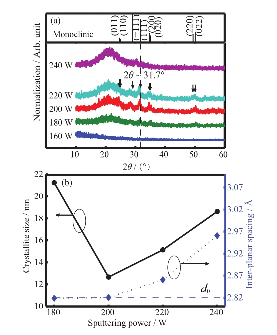
FIG.1(a)XRD spectra of HfO2films after 600oC annealing in oxygen ambient.(b)The calculated crystallite size and inter-planar spacing of annealed films at diflerent sputtering power.
where λ denotes X-ray wavelength(λ=1.5406 ?A)and θ denotes half angle of scattering vector corresponding to(111)peaks in XRD patterns. As shown in FIG.1(b),dfequals to 2.82,2.82,2.86,and 2.96?A,corresponding to sputtering power of 180,200,220,and 240 W,respectively.Compared with(111)standard inter-planar spacing(d0=2.82?A)for stress-free relaxed monoclinic hafnia system,the increase of inter-planar spacing causes negative sign of?d/df[22],which indicates compressive strain in these films.

It reveals that the crystalline quality which aflects film density is improved with RF power.The compressive stress can be caused by grain boundary densification[23,24]which attributes to atomic peening[25,26]and adatom oxygen diflusion into grain boundaries.FIG.1(b)also depicts the calculated average crystallite sizes of samples by applying the Scherrer equation[14]:
where L denotes the structural coherence length,λ denotes the wavelength of the X-ray radiation(0.1542 nm),θ denotes the half angle of scattering vector of(111)peak,Weffdenotes the eflective full width at half maximum(FWHM)of(111)peak after background subtraction and correction for instrumental broadening.The crystallite size aflects film density and the refractive index[13].More details about correlation between compressive strains,crystallite size,and refractive index will be discussed in the following of optical properties analysis.
B.XPS results
The XPS spectra of Hf 4f and O 1s for the samples asdeposited(a,c)and after annealing(b,d)are illustrated in FIG.2.After Shirley background subtraction,Hf 4f and O 1s XPS peaks are calibrated using C 1s peaks(284.8 eV)of the surface carbon contamination,having contrasted to the profile of C 1s,O 1s,and Hf 4f spectra reported in Refs.[13,15].In FIG.2(a)and(b),Hf 4f spectra are decomposed into two contribution of Hf 4f5/2and Hf 4f7/2with the spin-orbit splitting of 1.6 eV,which correspond to the Hf?O bond.
Before annealing,as shown in FIG.2(c),these main peaks(~530 eV)of O 1s are exemplified with decomposed Gaussian peaks,corresponding to Hf?O,exhibiting a blue shift which indicates the increase of Hf dangling bonds with sputtering power.Peak at 531.4 eV denotes water or?OH groups[27]and that at 532.9 eV denote C?O.After annealing,in FIG.2(d),the bonding energy of Hf?O at 530 eV indicates that stable Hf?O bonds are formed and plentiful hafnium dangling bonds are eflectively passivated[28].In addition,it can be noticed that C?O bonds almost disappear,and the intensity of physisorbed water or?OH decreases.
For all the samples as-deposited and after annealing,the stoichiometric ratio of O/Hf is evaluated by the intensities of oxygen(530 eV)to that of hafnium(17.1 and 18.7 eV)peaks.As depicted in FIG.3(a),O/Hf ratio of as-deposited films decreases with the increase of the sputtering power,which could be due to the broken Hf?O bonds and oxygen-deficiency.However,in spite of a minimum at 200 W,O/Hf ratio systematically increases for reduction of oxygen vacancy after annealing in 600oC oxygen ambience[29].
C.Optical constants
The growth rate and refractive index are derived from the experiment results of spectroscopic ellipsometer,according to Tauc-Lorentz model[30–35].The growth rates of films are approximately 3.0,4.4,6.2,4.2,and 1.1 nm/min under RF power from 160 W to 240 W.The increase of growth rate with power from 160 W to 200 W indicates more eflective bombardment of the target.As the power continues to increase from 200 W to 240 W,the growth rate decreases for the prominent re-sputtering process with limited mobility transition of sputtered partials to the film surface[19,20].Before the adatoms impact on substrate surface,the HfOxadatoms migrate parallelly to the incident beam.Upon impact,the adatoms keep a part of their momentum parallel to the substrate surface.This conservation of parallel momentum suggests that it might play a decisive role in the formation of the film structure.In our study,the incidence beam can also result in this mobility transition.However,the mobility transition should be weak,increasing the film density and reducing the optical adsorption.

FIG.2 XPS spectra of the samples by diflerent sputtering powers:(a)as-prepared Hf 4f,(b)Hf 4f after annealing in 600oC in O2,(c)as-prepared O 1s,and(d)O 1s after annealing in 600oC in O2.
After annealing,the thickness decreases with the lattice contraction for eflectively passivated hafnium dangling bonds in power range from 160 W to 200 W[36,37].And in power range of 220?240 W,thickness of annealed film increases slightly due to oxygen diflusion and crystallite size increases in annealed HfOxthin film[36].
The variation of stoichiometry and structural properties directly influences the optical characteristics of the samples[1].In FIG.3(a)and(b),as the sputtering power increases from 160 W to 200 W,the O/Hf ratio falls from about 1.7 to 1.4 and the growth rate increases from 3.0 nm/s to 6.2 nm/s,while the refractive index decreases,signifying that the film has less optical density.This result is due to surface dipole repulsion,which implies dominant repulsive force between Hf4+atoms and therefore reduction in oxygen atom[36].In addition,the increasing proportion of nonstoichiometric HfOx(x<2)with broken Hf?O bonds reduces the average dispersion energy parameter,which results in the reduction of refractive index in disordered HfO2films[15,20,38].A minimum refractive index of as-depositedfilms appears at power of 200 W.As the power goes up from 200 W to 220 W,the O/Hf ratio and the growth ratio decrease,refractive index increases for the reduction of film porosity by re-sputtering process.The thickness of as-deposited film at 240 W is just about 17 nm,and the roughness of the substrate could result in equivalent eflect of void between film and substrate and decrease detected refractive index at the same time.
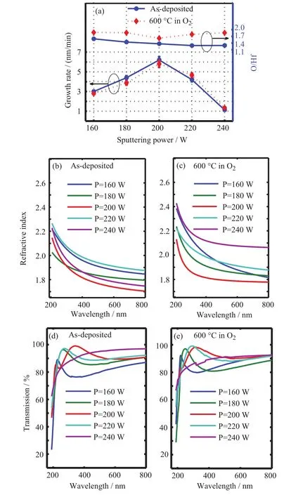
FIG.3(a)Thickness,O/Hf ratios of HfO2films before and after annealing.(b,c)Refractive index and(d,e)transmission spectra.
After annealing,refractive index in FIG.3(c)systematically increases with the improving of stoichiometry and density of monoclinic phase films[36]which are deduced from O/Hf ratios,crystallite size,and compressive stress.Hf dangling bonds are eflectively passivated,resulting in increase of attraction force between Hf4+and O2?dipoles and average dispersion energy parameter.Meanwhile,crystallite size decreases with O/Hf ratio within power from 180 W to 200 W and films keep in stress-free state.Then,as power goes up from 200 W to 240 W,the increase of crystallite size and the compressive stress in films enhances optical density[37]and refractive index.However,it could not be negligible that refractive index in the transition region(200?220 W)increases slightly after annealing.In consideration of the limited improvement of stoichiometry,this phenomena might be due to the minimum crystallite size and stress-free state,therefore,slight increase of optical density.
FIG.3(d)and(e)show transmittance spectra of all prepared HfO2films with low absorption in wavelength range above λ=200 nm.As depicted in FIG.3(c),these high values of transmittance at 200 and 220 W RF power are obtained for the density films with low porosity ratio,especially at 200 W.The low transmittance of the film with RF power below 180 W might be due to porosity in films for low kinetic energy of the ionic gas source[39].And after annealing,the increase of the samples transmittance,shown in FIG.3(e),would be attributed to the reduction of film porosity(increase of film density)and the optimization of stoichiometric ratios.Additionally,the increase of transmittance of the sample at 240 W could be due to the reduction of equivalent eflect of void between film and substrate and the increase of roughness which leads to the scattering of incident beam.
Considering the stability of films characteristics after annealing,especially the refractive index and optical transmittance,we choose annealed films which are deposited approximately at 220 W with the merits of moderate refractive index above 2 in UV band,high transmission and high film density,and apply these films to UV AR coatings.
IV.CONCLUSION
In this work,we have investigated ultraviolet optical and structural characteristics of RF-deposited HfO2thin films at diflerent sputtering power.After annealing,films show optimization of stoichiometric ratios for eflective passivation of hafnium dangling bonds and high optical density which is attributed to the growth of nanocrystalline.It can be found that the annealed HfO2films with sputtering power of about 220 W have high density,high transmission,and moderate refractive index.Therefore,the HfO2material is significant in the application as the high refractive index materials,which combines with low refractive index materials(SiO2or Al2O3)to form an optical antireflection coatings in UV wavelength.
V.ACKNOWLEDGMENTS
This work was supported by the Natural Science Foundation ofFujian Province ofChina(No.2018J05113) and the FundamentalResearch Funds for the Central Universities(No.20720160123,20720170013,and No.20720170084).
[1]G.He,Zh.Q.Sun,G.Li,and L.D.Zhang,Crit.Rev.Solid State Mater.Sci.37,131(2012).
[2]M.Vargas,N.R.Murphy,and C.V.Ramana,Opt.Mater.37,621(2014).
[3]V.Pervak,F.Krausz,and A.Apolonski,Thin Solid Films 515,7984(2007).
[4]P.Torchio,A.Gatto,M.Alvisi,G.Albrand,N.Kaiser,and C.Amra,App.Opt.41,3256(2002).
[5]S.Jena,R.B.Tokas,K.D.Rao,S.Thakur,and N.K.Sahoo,App.Opt.55,6108(2016).
[6]J.M.Yuan,L.Yuan,H.B.He,K.Yi,Z.X.Fan,and J.D.Shao,Appl.Surf.Sci.254,4864(2008).
[7]J.W.Zhang,G.He,L.Zhou,H.S.Chen,X.S.Chen,X.F.Chen,B.Deng,and J.G.Lv,J.Alloys Compd.611,253(2014).
[8]F.Zhang,W.F.Yang,H.L.Huang,X.P.Chen,Z.Y.Wu,H.L.Zhu,H.J.Qi,J.K.Yao,Z.X.Fan,and J.D.Shao,Appl.Phys.Lett.92,251102(2008).
[9]H.Angus Macleod,Thin-Film Optical Filters,4th Edn.,Boca Raton:Taylor&Francis,(2001).
[10]M.Scherer,J.Pistner,and W.Lehnert,Opt.Interfer.Coat.MA7(2010).
[11]J.Vlˇcek,A.Belosludtsev,J.Rezek,J.Houˇska,J.ˇCapek,R.ˇCerstv′y,and S.Haviar,Surf.Coat.Tech.290,58(2016).
[12]T.J.Bright,J.I.Watjen,Z.M.Zhang,C.Muratore,and A.A.Voevodin,Thin Solid Films 520,6793(2012).
[13]S.S.Lin and H.R.Li,Cer.Inter.39,7677(2013).
[14]M.Y.Ho,H.Gong,G.D.Wilk,B.W.Busch,M.L.Green,P.M.Voyles,D.A.Muller,M.Bude,W.H.Lin,A.See,M.E.Loomans,S.K.Lahiri,and Petri.I.R¨ais¨anen,J.Appl.Phys.93,14771(2003).
[15]C.V.Ramana,M.Vargas,G.A.Lopez,M.Noor-AAlam,M.J.Hernandez,and E.J.Rubio,Cer.Inter.41,6187(2015).
[16]V.Dave,P.Dubey,H.O.Gupta,and R.Chandra,Thin Solid Films 549,2(2013).
[17]G.Aygun,A.Cantas,Y.Simsek,and R.Turan,Thin Solid Films 519,5820(2011).
[18]V.Dave,P.Dubey,H.O.Gupta,and R.Chandra,Proceedings of American Institute of Physics,United States,1576,29(2014).
[19]L.Abelmann and C.Lodder,Thin Solid Films 305,1(1997).
[20]S.H.Wemple,J.Chem.Phys.67,2151(1977).
[21]M.Ladd and R.Palmer,Structure Determination by X-ray Crystallography,4th Edn.,Kluwer Academic/Plenum Publishers,New York,117-175(2003).
[22]S.Jena,R.B.Tokas,J.S.Misal,K.D.Rao,D.V.Udupa,S.Thakur,and N.K.Sahoo,Thin Solid Films 592,135(2015).
[23]C.Pao,S.M.Foiles,E.B.Webb III,D.J.Srolovitz,and J.A.Floro,Phys.Rev.Lett.99,036102(2007).
[24]E.Chason,B.W.Sheldon,L.B.Freund,J.A.Floro,and S.J.Hearne,Phys.Rev.Lett.88,156103(2002).
[25]J.A.Thornton and D.W.Hoflman,Thin Solid Films 171,5(1989).
[26]C.A.Davis,Thin Solid Films 226,30(1993).
[27]Y.J.Wang,Z.L.Lin,X.L.Cheng,H.Xiao,F.Zhang,and S.C.Zou,Appl.Surf.Sci.228,93(2004).
[28]S.C.Chen,C.C.Ting,H.H.Su,P.C.Yang,J.Lu,H.C.Huang,D.S.Gan,N.J.Ho,and Y.Shi,Mater.Lett.63,1914(2009).
[29]W.T.Liu,Z.T.Liu,F.Yan,T.T.Tan,and H.Tian,Surf.Coat.Tech.205,2120(2010).
[30]G.E.Jellison Jr.and F.A.Modine,Appl.Phys.Lett.69,371(1996).
[31]G.E.Jellison Jr.and F.A.Modine,Appl.Phys.Lett.69,2137(1996).
[32]J.Jaiswal,S.Mourya,G.Malik,S.Chauhan,A.Sanger,R.Daipuriya,M.Singh,and R.Chandra,Appl.Opt.55,8368(2016).
[33]J.Jaiswal,S.Mourya,G.Malik,and R.Chandra,J.Opt.Soc.Am.A 35,740(2018).
[34]G.Malik,J.Jaiswal,S.Mourya,and R.Chandra,J.Appl.Phys.122,143105(2017).
[35]S.Mourya,J.Jaiswal,G.Malik,B.Kumar,and R.Chandra,J.Appl.Phys.123,023109(2018).
[36]S.Pandey,P.Kothari,S.K.Sharma,and K.J.Rangra,J.Mater.Sci.27,7055(2016).
[37]F.Parmigiani,E.Kay,T.C.Huang,and J.D.Swalen,Appl.Optics 24,3335(1985).
[38]S.Goldsmith,E.C?etin¨org¨u,and R.L.Boxman,Thin Solid Films 517,5146(2009).
[39]L.Abelmann and C.Lodder,Thin Solid Films 305,1(1997).
 CHINESE JOURNAL OF CHEMICAL PHYSICS2018年6期
- CHINESE JOURNAL OF CHEMICAL PHYSICS的其它文章
- Imaging HNCO Photodissociation at 201 nm:State-to-State Correlations between CO(X1Σ+)and NH(a1?)
- Energy-Transfer Processes of Xe(6p[1/2]0,6p[3/2]2,and 6p[5/2]2)Atoms under the Condition of Ultrahigh Pumped Power
- Ultrafast Investigation of Excited-State Dynamics in Trans-4-methoxyazobenzene Studied by Femtosecond Transient Absorption Spectroscopy
- Strong Current-Polarization and Negative Diflerential Resistance in FeN3-Embedded Armchair Graphene Nanoribbons
- Unexpected Chemistry from the Homogeneous Thermal Decomposition of Acetylene:An ab initio Study
- Direct Observation of Transition Metal Dichalcogenides in Liquid with Scanning Tunneling Microscopy