
Dislocation slip behaviors in high-quality bulk GaN investigated by nanoindentation
2021-11-23 07:29KaiHengShao邵凱恒YuMinZhang張育民JianFengWang王建峰andKeXu徐科
Chinese Physics B 2021年11期
Kai-Heng Shao(邵凱恒) Yu-Min Zhang(張育民) Jian-Feng Wang(王建峰) and Ke Xu(徐科)
1School of Nano-Tech and Nano-Bionics,University of Science and Technology of China,Hefei 230026,China
2Suzhou Institute of Nano-Tech and Nano-Bionics,Chinese Academy of Sciences(CAS),Suzhou 215123,China
3Suzhou Nanowin Science and Technology Co.,Ltd,Suzhou 215123,China
Keywords: GaN,dislocation,nanoindentation,cathodoluminescence,TEM
1. Introduction
GaN, as a III-V semiconductor, has attracted much attention because of its wide bandgap of 3.4 eV that has led to its wide application in optical and electronic devices.[1,2]Employing high-quality bulk GaN substrates makes semiconductor devices exhibit much better performances.[3,4]Investigating the formation and movement of dislocations in GaN crystals is essential to further reduce the dislocations in GaN substrates. Study of mechanism of dislocation movement could help optimize the GaN devices manufacturing process since operation caused degradation can be prevented.
Nanoindentation is a useful method to study dislocation formation and movement in GaN single crystals. In previous nanoindentation experiments, the pop-in found on the load curve was considered as dislocation homogeneous nucleation.[5,6]which is associated with elastic-plastic transition point.[7]It is generally accepted that the{0001}basal plane is a primary dislocation nucleation plane after pop-in event.[8-10]When it comes to nucleation on a pyramidal plane,experimental conclusions are inconsistent. Jahnet al.[11]used both Vicker indenter and Berkovich indenter to induce indentation onc-GaN,and only the slip system of〈11-20〉{1-100}was observed. Although the indenters used were different,Bradbyet al.,[10]Jian,[12]and Huanget al.[13]found dislocation slips on both{0001}plane and{10-11}plane. Fujikaneet al.[14]concluded that slips would nucleate on the{0001}plane,{10-10}plane,and{10-12}plane. Qianet al.[15]conducted a series of molecular dynamics simulations and found that slips nucleate on{10-10}plane,{0001}plane,{10-12}plane,and{10-11}plane.
During the experiment, the dislocation of crystal affects the induced-dislocation formation process. In this study,nanoindentations are induced on a high-quality bulk GaN crystal and thus the results obtained turns different from those reported in previous papers. We confirm the pyramidal plane by the method reported and explain the novel phenomenon by the dislocation intersection theory.
2. Experiment
Nanoindentation experiments were performed on a 325-μm-thick freestanding GaN bulk crystal grown by hydride vapor phase epitaxy (HVPE). The dislocation density of the GaN was 8.62×104cm?2characterized by cathodoluminescence(CL).Nanoindentation tests were performed on the GaN{0001}surface using a nanoindentation system(Nano Indenter G200) while the strain rate was set to be 0.05 s?1. A Berkovich indenter with a radius of curvature of 50 nm and a conical indenter with a radius of curvature of 4.9μm were both employed in experiments on indentation. Repeated indentations reached a depth of 1000 nm while the interspace between two points was 50 μm by Berkovich indenter and conical indenter separately.Because the penetration depth was 1000 nm,conical indenter could be considered as a ball indenter while Berkovich indenter’s peak could be ignored. Scanning electron microscopy (SEM)-CL system was used to characterize the indentations’ surface area. We selected a conical indenter to create indentations. When the pop-in just occurred because its curvature radius is big enough,the induced indentations were homogeneous. The focus ion beam(FIB)was used to prepare the samples of ‘pop-in’ indentations where initial plastic deformation was for cross-sectional transmission electron microscope (TEM). The CL images were taken before and after inductively coupled plasma etch(ICP)had conducted on the same indentation. It was helpful to confirm the threedimensional model of dislocation orientation.
3. Results and discussion
Figure 1 shows a typical load-displacement curve ofcplane GaN bulk loaded up to a maximum depth of 1000 nm with two tips. Discontinuity on the loading curve(pop-in only found once during the indentation) is found at 0.5 mN and 50 mN with Berkovich indenter and conical indenter respectively.Pop-in occurs later with the indenter’s radius increasing because the stress concentration is weaker.
Figures 1(b)and 1(c)show nanoindentation with a maximum depth of 1000 nm onc-plane characterized by CL.The CL images are the projection of the slipped dislocations onto plane{0001}.Six slip bands(three pairs)are consistent distribution along the〈11-20〉zone axis in Figs.1(b)and 1(c)where indentations are created by conical indenter and Berkovich indenter respectively. Besides the cross band being consistent with previous papers, dislocation loops are found in CL images.Interestingly,the observed dark circular arcs(dislocation loops)are cut along the〈11-20〉axis and〈1-100〉axis. Independent of the indenter,12 dark circular arcs exist further away from the indentation than cross bands. All phenomena are in good consistence with the hexagonal symmetry. It is worth noting that bright luminescence along the〈11-20〉axis and〈1-100〉axis is also consistent with the hexagonal symmetry well. The dislocation density of the GaN is 8.62×104cm?2under the consideration of the scaled(indentation affected area size is 50 μm×50 μm) indentation which can be thought as being induced on an approximate-perfect crystal.

Fig. 1. (a) Load-displacement curve on c-plane from conical indenter and Berkovich indenter, [(b), (c)] room-temperature panchromatic CL images of indentations in c-plane GaN:maximum depth 1000 nm,CL accelerating voltage 5 kV,(b)conical indenter,(c)Berkovich indenter.
To confirm the slip bands existing in the pyramidal plane,we create ‘pop-in’ indentations for further research. The CL characterization shows that the depth of nanoindentation does not influence the dislocation pattern distribution,which means that the slips occur at the beginning of plastic deformation.Bright luminescence along the〈11-20〉and〈1-100〉axes are considered as vacancy luminescence[16]in the monochromatic CL(400 nm)images(Fig.2).
Figure 2 shows the CL images of indentation at the point of elastic deformation to plastic deformation by conical indenter. Figures 2(a)-2(d) are panchromatic CL images and figures 2(e)-2(h) are monochromatic CL images collected at 400 nm. Dislocation loops and slip bands are observed from the CL images and it is possible that there can be two dislocation nucleation planes because the indentation is induced at the point of plastic deformation. Interestingly, dislocation loops and vacancy luminescence are collected more and more with the accelerating voltage (proportional to depth) increasing. Notably, both loops and luminescence can rarely be collected when accelerating voltage is low. The surface state of the crystal will be a reasonable explanation for why the dislocation loops and dislocation luminescence cannot be found at the surface. Dislocation loops are cut apart along the〈11-20〉axis and the〈1-100〉axis, and the vacancy luminescence is also observed along the〈11-20〉axis and the〈1-100〉axis,which means that the dislocations on different planes intersect along these axes (or projection on{0001}along these axes). To further verify the assumption,the cross-section sample needs characterizing.
The cross-sectional TEM sample are prepared by FIB(the green line in Fig. 3(a)). The STEM image of the pop-in indentation is shown in Fig.3(b). The comparison of the angle betweenc-plane and pyramidal cross band with the theoretical angle confirms that the cross band is on{10-11}pyramidal plane, which is consistent with the result in precious papers.[10,12,13]

Fig.2. Room-temperature CL images of a conical indentation in c-plane GaN:maximum load 55 mN[(a)-(d)]panchromatic CL,accelerating voltage 2 kV,5 kV,10 kV,15 kV,respectively;[(e)-(h)]monochromatic CL,accelerating voltage 2 kV,3 kV,5 kV,15 kV,respectively,
It is worth noting that in the{11-20}plane, dark spots are observed along the sloping dark lines ({10-11}pyramidal slip bands) in Fig. 3(b). Besides, in the{0001}plane,the dark spots are also found along line〈11-20〉in CL images ofc-plane(Figs.1 and 2). Analyses of the projection on{0001}plane and{11-20}plane confirm that the dislocations on{10-11}pyramidal slip bands are dislocation loops. Dislocation loops on{0001}slip band can be confirmed in a similar way.
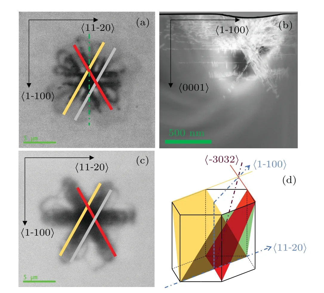
Fig.3. (a)Room-temperature panchromatic CL image of pop-in indentation by conical indenter; (b)dark field STEM acquired along 〈1-100〉 zone axis by FIB;(c)room-temperature panchromatic CL image before and after ICP etching;(d){10-11}pyramidal plane specific orientation(yellow,red,gray in accord with panels(a)and(c)).
To clear specific pyramidal plane orientation,the CL images are taken before and after ICP etching. Figures 3(c)and 3(d)indicate that two separate{10-11}pyramidal bands along the same direction in the photo (marked as yellow line and gray line, respectively) intersect along the〈11-20〉direction.This indicates that a pair of parallel (from the projection of{0001})slip bands’orientations look like Fig.3(d). Further,a pair of slip bands’ orientations (marked red and yellow in Fig. 3(c), respectively) is also shown. Notably, the intersection between the yellow bands and the red bands is〈-3032〉,of which the projection on{0001}is〈1-100〉. Unlike the pair of yellow slip band and gray slip band,the intersection between the yellow band and the red band exists only at the position closest to the indentation while the intersection between the yellow and grey bands exists far away from indentation.
Figure 4 contains schematic diagrams of dislocation intersection happening between dislocation loops on{0001}and{10-11}panels. It is generally accepted that two single dislocations can react when they move and meet at a point. Depending on the burger vector of dislocation, at the point of intersection can occur different reactions, leaving either kink or jog. After the intersection, dislocation with jog will leave vacancies along the movement direction when dislocation continues to move.
Figures 4(a)-4(c) illustrate the dislocation intersections of loops on{0001}and{10-11}. Dislocation loops are found to be circular arcs(Figs.1 and 2)because dislocation loops on{0001}are cut off along the〈11-20〉direction after processes(a)-(c). The trail of vacancies along the〈11-20〉direction(CL image in Fig.2)proves the intersection process. Near the indentation, there exists a〈-3032〉line of steps created by two{10-11}slip bands,which is mentioned in Fig.3(d). Dislocation loops on{0001}will get intersected and leave a trail of vacancies along the〈1-100〉direction when expanding. Notably,a dark line is also left because both jog and kink are left on it when{0001}dislocations get intersected.[17]
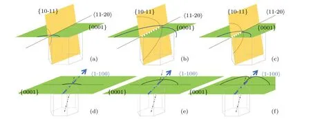
Fig. 4. Schematic diagrams of dislocation intersection: [(a)-(c)] intersection happening between dislocation loops on {0001} and {10-11};[(d)-(f)]intersection between〈-3032〉step line and dislocation loops on{0001}.
4. Conclusions
The high-quality bulk GaN makes it possible to focus on the natural deformation under nanoindentation without considering threading dislocations. Based on the dislocation intersection theory,vacancy luminescence and dislocation loops in hexagonal symmetry are explained. Dislocation loops on{0001}are cut off along the〈11-20〉direction and〈1-100〉direction by dislocations on{10-11}and〈-3032〉step lines,respectively. Vacancies are left along〈11-20〉direction and〈1-100〉direction when the original dislocation expands after the intersection.

- Chinese Physics B的其它文章
- Numerical investigation on threading dislocation bending with InAs/GaAs quantum dots*
- Connes distance of 2D harmonic oscillators in quantum phase space*
- Effect of external electric field on the terahertz transmission characteristics of electrolyte solutions*
- Classical-field description of Bose-Einstein condensation of parallel light in a nonlinear optical cavity*
- Dense coding capacity in correlated noisy channels with weak measurement*
- Probability density and oscillating period of magnetopolaron in parabolic quantum dot in the presence of Rashba effect and temperature*