
Stress distribution variations during nanoindentation failure of hard coatings on silicon substrates
2024-01-08 13:04RitambharaDashKushalBhattacharyyaandArnabBhattacharyya
納米技術與精密工程 2023年4期
Ritambhara Dash,Kushal Bhattacharyya, and Arnab S.Bhattacharyya,3,a)
AFFILIATIONS
1 Department of Metallurgical and Materials Engineering,Central University of Jharkhand,Ranchi 835205,India
2Department of Mechanical Engineering,Netaji Subhash Engineering College,Kolkata 700152,India
3Centre of Excellence in Green and Efficient Energy Technology(CoE GEET),Central University of Jharkhand,Ranchi 835205,India
ABSTRACT Regarding quality inspection of technologically important nanocomposite hard coatings based on Ti,B,Si,C,and N and bioceramics such as hydroxyapatite that are used in small-scale high-precision devices and bio-implants,it is essential to study the failure mechanisms associated with nanoindentation,such as fracture,delamination,and chipping.The stress imposed by the indenter can affect the fracture morphology and the interfacial fracture energy,depending on indenter shape,substrate type,crystallographic properties,pre-existing flaws internal microcracks,and pre-strain.Reported here are finite-element-base fracture studies that provide insights into the different cracking mechanisms related to the aforementioned failure process,showing that the fracture morphology is affected by the interaction of different cracking events.The interfacial fracture energy,toughness,and residual stress are calculated using existing models with minor adjustments,and it is found that increasing the indenter sharpness improves the shear stress distribution,making the coating more prone to separation.Depending on the prevailing type of stress,the stress distribution beneath the depression results in either crack formation or a dislocation pile-up leading to strain hardening.Different forms of resistances resulting from the indentation process are found to affect the tip–sample conduction,and because of its stronger induced plasticity than that of a Berkovich indenter tip,a sharper cube-corner tip produces more resistance.
KEYWORDS Nanoindentation,Hard film,Finite-element analysis (FEA),Cracking mechanism,Stress
I.INTRODUCTION
Nanoindentation is used extensively for the nanomechanical characterization of materials used in microelectronics.Nanocomposite hard coatings comprising phases such as SiC,Si3N4,CNx,TiC,TiN,TiB2,and cBN have applications in the fabrication of nano/microelectromechanical systems (N/MEMS) devices,interconnects,and metallurgical protective coatings,and biomaterials such as manufactured (prosthetics and bio-implants) and natural (bone,tissue,etc.) ones are also being used in nanoindentation.Obtaining attributes such as hardness,decreased modulus,fracture toughness,adhesion,and wear from nanoindentation depends on making contact between the indenter tip and the material being studied,1,2and assessing fracture behavior is important when considering the durability of these coatings in adverse conditions or being subjected to external stimuli for fil failure.3,4
Begun by Hertz in 1881,the study of indentation-based fracture has developed over the years,such as with the energy-based criterion due to Griffit and the energy balance analysis due to Frank and Lawn.5–12The mechanisms behind the different cracking phenomena that occur in micro/nanoindentation using indenters of different shapes have been analyzed and reported extensively over the years.13–16
For coated samples,the fracture mode depends on the coating thickness and the indenter geometry.A sharper indenter causes more plastic deformation,with mode-I fracture more prevalent for a higher ratio of tip radius to sample thickness.The nature of the substrate and interface and the load applied also affect the fracture morphology for coated systems.The cracked segments also experience multiple minor cracks and branches because of stress relaxation after indentation(load withdrawal),and coatings subjected to indentations by smaller indenters are found to be more prone to interfacial failure.17–21The stress imposed by the indenter affects the fracture nature depending on the coating’s mechanical and crystallographic properties and the existence of any pre-existing flaws internal micro-cracks,and pre-strain.Plate or membrane bending models have been used for Hertzian (spherical) contacts,22–25and the stress distribution and determination of interfacial fracture associated with hard pyramidal indenters have been reported based on models proposed by den Toonderet al.,4Bull,14and Thouless.26
In fracture investigations of film/substrat systems,crack-based stress intensities are transferred to the substrate,resulting in various cracking events,including radial(palmist),median,half-penny,lateral,secondary palmist,and shallow lateral cracks.3Radial cracks are related to fracture toughness and so have been used to estimate it using crack-opening-displacement models.Lateral cracks,fil delamination,and chipping show how the substrate is also implicated,as are the adhesive capabilities of the films Additionally,methods based on geometric mapping of the chipped region as well as an energy-based technique have been published for determining the interfacial toughness.3,4,14,27The stress distribution during fracture caused by indentation is so complicated that it demands further in-depth analysis.Finite-element analysis(FEA)has been used previously to determine the fracture toughness and trajectories of cracks using extended finite-elemen modeling (FEM),the cohesive zone model (CZM),and the virtual crack closure technique.However,the different approaches must be combined to assess mixed-mode fractures.28,29Herein,we seek to enrich this area of study by correlating the fil failure phenomena with FEA and trying to understand the interactions among different cracking phenomena.
II.MATERIALS AND METHODS
Hard film of the nanocomposites SiCN and TiB2were deposited on silicon substrates by RF magnetron sputtering(HINDHIVAC,Bangalore)using 2-in.sintered ceramic targets of SiC and TiB2with a supply of argon and nitrogen gas,the details of which have been reported previously.30,31The nanoindentation tests were performed using nanoindenters(MTS,USA)in the form of a threesided pyramidal Berkovich indenter and a cube-corner indenter.Images of the nanoindented regions were captured using an optical microscope(LEICA Microsystems,Germany).
FEA was performed using ABAQUS 6.13,with 3D FEM of quarter specimens because of symmetry and to reduce the computational time.The boundary conditions used in the model are shown in Fig.1(a).Eight-node isoparametric hexahedral elements with eight Gauss points were used for the calculations,and reduced integration was done with full Newtonian nonlinear analysis computation for all the specimens.The mesh was refine with an element volume of 0.0002×0.0002×0.0002 mm3in the region ahead of the indenter,and the element size was kept constant near the crack tip to facilitate calculation of the stress distribution.
In total,38 360 linear hexahedral elements of type C3D8R were used for the analysis.Elastic-plastic FEA was performed using ABAQUS 6.13,and the Young’s modulusE,Poisson’s ratio,and yield stress vs plastic strain required for the FEA were obtained from the nanoindentation tests.The material behavior for the analysis was isotropic elastic and isotropic hardening plastic.To induce the large strain expected in the indenter tip,large-deformation theory was used.The mesh distribution is shown in Fig.1(b).The indenter was taken as a discrete rigid object,and surface-to-surface contact was established between the indenter and the film The indenter surface was considered as the master surface,and the fil was considered as the slave surface.The discretization method was node to surface.A reference point was created on the indenter through which displacement was provided.
III.RESULTS AND DISCUSSION
A.Shear stress distribution and failure
Figure 2 shows the distribution of shear stress (σxy) obtained from FEA [Fig.2(a)] and the fracture region showing different cracking and fil failure phenomena[Fig.2(b)].A schematic of the indentation-chipped segment showing the geometrical parameters required for estimating the interfacial fracture energy as per the proposed models is shown in Fig.3(a).The fracture features that occurred during the indentation process as observed in Fig.1(b)are shown schematically in Fig.3(b).Different types of cracks such as radial (r1),lateral (L1,L2),secondary radial (r2),and edge (e1,e2) were observed and marked.The mechanisms of cracking phenomena for radial(Palmqvist),secondary radial,and lateral cracks as shown in Figs.3(c) and 3(d) have been reported previously,3but some novel features were observed in addition to the aforementioned cracking.The indentation mechanism is a hybrid of radial and lateral cracks,and edge cracks may be observed to be developing on both surfaces.These result from a pre-existing fault that causes cracks to expand when loads are applied.Delamination occurs before the phenomena of chipping.The chipped segment C1 in Fig.2(b)is surrounded by delamination.The delaminated(going to be chipped) regions C2 and C3 are due to edge cracks and not lateral cracks.The interaction between the radial and lateral cracks causing the bending of the radial crack toward the delaminated region is shown schematically in Fig.3(d).
The shear stress distribution found via FEA can be related to the fracture shape.The sample encounters a sharp tip,inducing plastic deformation,and this causes the maximum stress area directly below the indentation.However,there are surrounding regions of hydrostatic stress(σhydro),which is expressed as
whereσx,σy,andσzare the normal stresses in theX,Y,andZdirections.This hydrostatic stress can also cause phase transformation in the silicon substrate.At the interface,the shear components of the hydrostatic stress are important because they add to the pre-existing residual stress (σres) due to the difference in the material configu ration of the fil and substrate,causing fil failure after a certain threshold value.
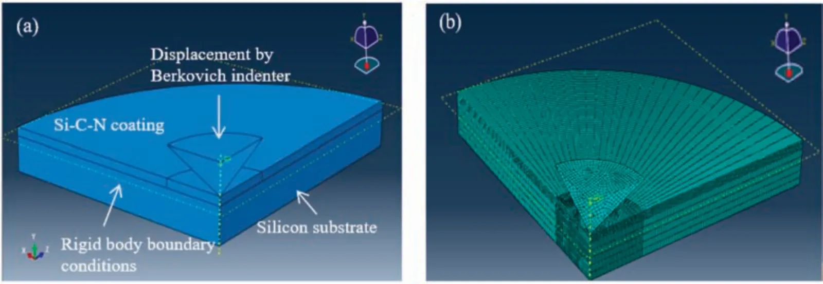
FIG.1.(a)Quarter model showing boundary conditions,and(b)mesh distribution of quarter specimen.
B.Interfacial fracture energy
The radial(Palmqvist)crack occurs in the coating region,and the stress distribution is confine to a small region and eventually moves to the surface.The radial crack—which is a measure of toughness—is seen to deviate from its linear path,indicating good toughness due to the formation of nanocrystallites during the fil deposition process.31The interfacial region is very important in the case of the lateral crack,which is related to fil adhesion and wear.A clear demarcation in the flo ofσhydrocan be seen at the film–substrat interface.The stress is seen to take a path along the interface and is transferred to the substrate,from the load applied to the specimen creating lateral cracks.This inhomogeneity in stress distribution becomes more severe and leads to delamination and eventually chipping.The geometrical parameters of the chipped segment as shown in Fig.2(b)can be used to determine the interfacial fracture energy as3,4,14,26,27
Approximate estimates of the interfacial energies of the different zones were calculated as per Eq.(2) using the parameters obtained from the figure and given in Table I.The coating thickness wast=1.5 μm,Poisson’s ratio wasν=0.25,and the elastic modulus wasE=200 GPa.The firs term in Eq.(2) is very large and is the dominant term for the result,so the other terms were neglected for the calculations.Note that 1 GPa μm is equivalent to 1 kJ/m2,the unit of interfacial fracture energy.The calculated values show that the interfacial fracture energy was 59 J/m2for the chipped segment C1 and 68 J/m2for C4.The residual stress causing fil failure can be evaluated approximately fromΓiby dividing it byL,giving values of 5.9 and 5.7 GPa for C1 and C4,respectively.The interfacial modulus(Ei)and toughness(Kic)can also be determined as3
whereEcandEsare the modulus of the coating and substrate,respectively,which were 200 GPa for SiCN and 140 GPa for silicon,giving an interfacial modulus of 167 GPa.The interfacial fracture toughness was more than 3 MPafor C1 and C4.Another way of determining the fracture toughness is by applying3
wherePc(100 mN)is the critical load for generating a lateral crack,HandEare the hardness and modulus,respectively,andθis the indenter half-angle,which is 35○for the Berkovich indenter,giving a similar value of fracture toughness of ~3 MPa
Pre-existing tensile stress promotes adhesive failure via chipping,while compressive stress helps more in radial cracking.For a coating–substrate system,a modifie form of Stoney’s equation can be used,32i.e.,
wherehis the thickness of the total film–substrat system,andtis the coating thickness.The parameterDis the diameter of the coating considering the shape to be circular and is taken as 1 cm.The deposited fil was 1-μm thick on a 1-mm-thick Si substrate,sohis considered as 1 mm.The value of the spring constantkis taken as the stiffness 0.1 mN/nm(MN/m),giving a surface stress of 300 MPa,which increases on application of indentation.
In a coating–substrate system,through-thickness fracture and interfacial delamination give information about the coating toughness and adhesion,respectively.The residual stressσresin the coating is related to the interfacial toughness as given by33
whereβis a constant equal to 0.016,EandHare the modulus and hardness,respectively,Pis the applied load (~100 mN),andcis the crack length (15 μm).ConsideringKc=3 MPagivesσres=667 MPa.A shape factor is also included as given by3

TABLE I.Parameters for calculation of interfacial energy from chipped segments.
where the additional parameterdis the depth of the radial crack,which we take instead as the crack width [3 μm as shown in Fig.2(b)],givingZ=0.33.
For the interfacial fracture toughness for a plane-strain mode-I fracture,the energy-based model gives
whereUfis the fracture dissipated energy andAfis the fracture area,givingσres=4 GPa,which is close to the value in Table I.According to Griffith’ criterion,the total energy release rate (G) for a crack in a coating subjected to mode-I and mode-II loading is given byG=GI+GII,where
Crack extension occurs in the direction in which the total energy release rate is maximum and takes place when the maximum energy release rate reaches a critical valueGcgiven bywhich from pure mode-I loading isGc=45 J/m2for plane stress(α=1).

FIG.3. Schematics of (a) indentation-chipped segment showing geometrical parameters required for estimating interfacial fracture energy as per proposed models,14 (b)fracture features occurring during indentation process as observed in Fig.1(b),and mechanisms for(c)radial(Palmqvist)and lateral cracks and(d)edge cracks and interaction between radial and lateral cracks causing bending of radial crack.
C.Compressive and shear stress distributions
Figure 4(a) shows the FEA-determined stress distribution for a 1-μm-thick TiB2coating on a silicon substrate using a cubecorner indenter.The strain regions arising during nanoindentation are due to the tensile and compressive fields The tensile fiel exists in the firs region,which makes it expand in-plane without getting deeper horizontally.The region below it has compressive stress,which causes more in-depth expansion than lateral and touches the coating–substrate interface.In Fig.4(b),the compressive and shear stress distributions are plotted with respect to the displacement of the tip from the contact point into the film The results show a higher variation of the compressive stress along the axis of indentation,with a slope of 80 MPa/nm compared 40 MPa/nm for the shear stress.The shear stress was prevalent parallel to the film–surfac interface,increasing the chances of coating detachment.
Different types of cracking phenomena can occur during the indentation process,especially when using a sharp indenter such as the pyramidal Berkovich indenter or the cube-corner indenter.The equivalent cone angle associated with the Berkovich indenter is 70.3○(half-angle 35.15○),which becomes 42.23○for the sharper cube-corner indenter[Fig.4(c)].The stress distribution is different for the two cases.The influenc of pre-existing microcracks in the sample is somewhat mitigated by increased sharpness,which also lessens the through-thickness lateral cracking in the coating.The radial cracking is linked to fil toughness,whereas the lateral cracking is linked to the coating’s adhesion and wear resistance.Greater shear stress generation parallel to the fil substrate interface results from greater sharpness,increasing the likelihood of the fil separating from the substrate.The radial cracking occurs on the fil and is influence negligibly by the substrate,whereas the substrate is an important factor for lateral cracking,which causes the coating to detach from the substrate.For sharper indenters,however,the radial cracking becomes more dominant in causing fil failure,the experimental evidence for which has been reported earlier.30,34
FEM using the CZM has been used to study thin-fil failure processes such delamination and interfacial fracture related to coating adhesion,which is an important parameter for the performance of microelectronic devices.As discussed above when considering interfacial adhesion,the interfacial fracture energy release rate is affected by the stress distribution that develops beneath the indentation.35Nanoindentation and stress analysis have also been done for SAC(Sn–Ag–Cu)lead-free solder joints used in electronic packaging.36The fractured or heavily plastically deformed regions also influenc the electrical properties because they indicate high strain field surrounding the indentations,which interfere with the flo of free electrons.An influenc of the electric fiel on nanoindentation due to competition between mechanical load and electric fiel in the domain switching process has been reported,37,38and an effect of charge states on the yield and elastic modulus was obtained via stress–strain plots based on nanoindentation using the power-law hardening model for LixSn alloys.39
D.Tip conduction
Because current can pass through the contact region of the indenter and sample surface,the resistivity encountered by the current varies with the applied force causing plastic deformation.Plastic deformation is a major contributor to resistivity,which is very well established as dislocations acting as scattering centers for electrons.The resistanceRof the contact region has two contributions,i.e.,R=Rc+Rf,whereRcis the constriction resistance and depends on the bulk properties,andRfis the contact resistance due to the surface layer.39
This shows that the constriction resistanceRc(C)with the cubecorner indenter is three times the constriction resistanceRc(B)with the Berkovich indenter.A sharper indenter also causes a higher degree of plastic deformation,leading to the material being strain hardened in a localized zone surrounding the indentation region.
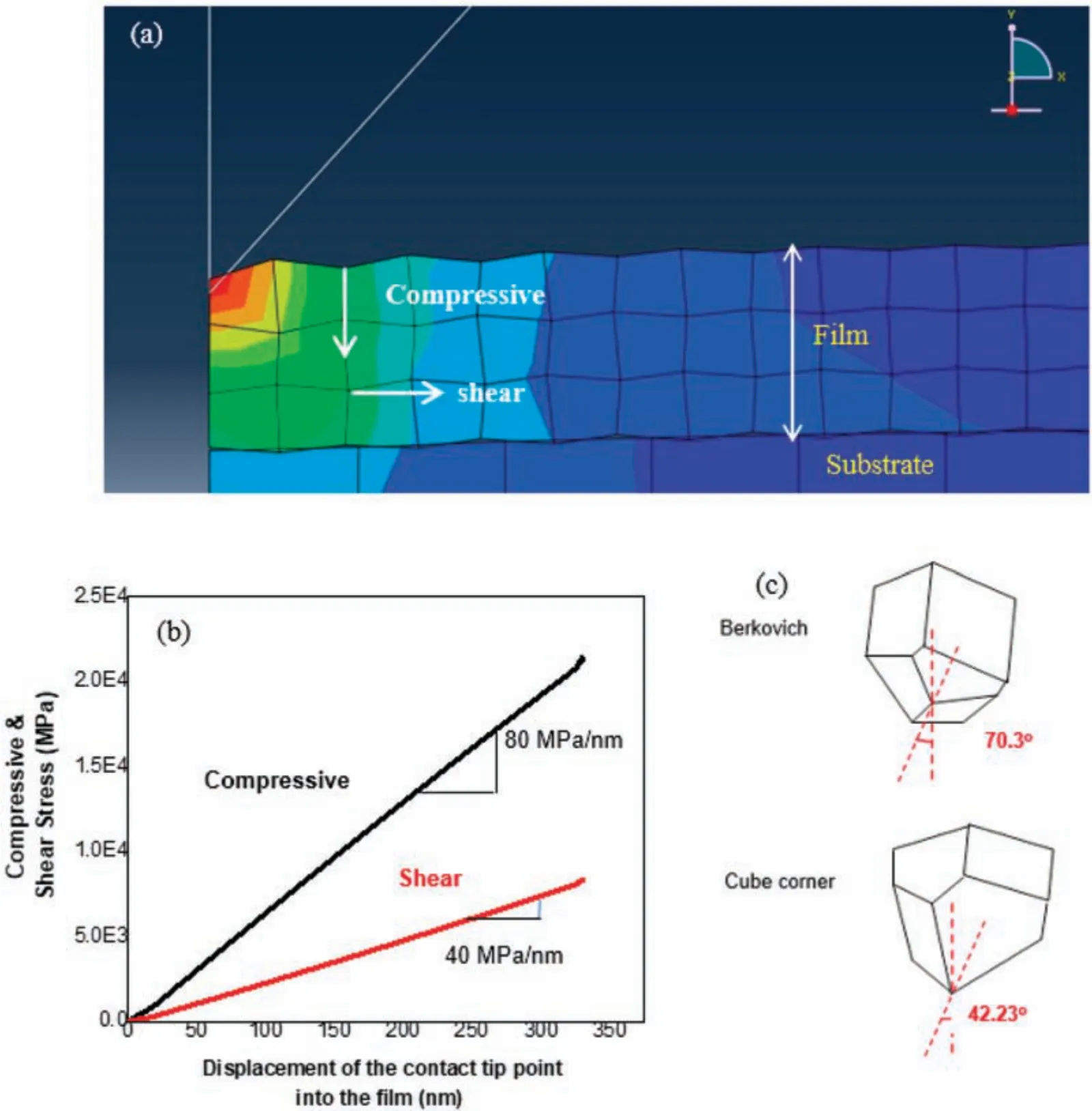
FIG.4.(a).Results of finite-elemen modeling(FEM)of nanoindentation of TiB2 coating on Si substrate.(b)Distributions of compressive and shear stress.(c)Geometries of Berkovich and cube-corner indenters.
The plastic zone near the crack tip is the dislocation distribution area with dimensionrc=,40whereΓiis the interfacial fracture energy and is taken as being 65 J/m2as an average of the values obtained previously (Table I).The parameterH(~20 GPa) is the hardness,givingrc=1 nm for the Berkovich indenter.Because of the higher indentation sharpness due to the projected areas being different,the plastic-zone radius for the cube-corner indenter is 9 nm,which again shows that dislocations piling up around a crack tip and causing strain hardening is much more prevalent with the sharper cube-corner indenter than with the Berkovich indenter.The constriction resistanceRc(B)being smaller thanRc(C),the tip voltage will be much higher with the Berkovich indenter than with the cube-corner indenter when used as a conducting tip and also as a MEMS nanoindenter with an integrated AFM cantilever gripper for nanomechanical characterizations,as in transducers for biosensing.41
For conduction to take place between the indenter tip and sample surface,an external bias is applied with the current direction as shown in Fig.5(a)(inset,top).The constriction resistanceRcand the contact resistanceRfare those that are affected by the indentation and any related phenomena.42The red dotted lines indicate the current flow which constricts at the contact causingRcand is affected by indentation as per Matthiessen’s rule,which states the contribution of deformation (plastic) in conduction.In addition toRc,the other resistance component that is affected by mechanical stimulus from the indenter in the case of a film–substrat system is the resistanceRintfat the coating–substrate interface,which may not be active at shallow indentation depths(less than 10%of the thickness).

FIG.5.(a) Electrical conduction between indenter tip and sample with different resistances with load depth and time on sample plot showing pop-in due to fracture.(b)Determination of energy dissipated due to fracture.(c)AFM image of the indentation region with line profil of one of the radial cracks showing its(d)area and(e)depth.
E.Pop-in events
Nanoindentation performed on TiB2film on silicon substrates showed fracture events as represented by pop-in in the load–depth plot[Fig.(5a)].The maximum shear stressτmaxand the maximum tensile stress induced during the indentation process at the point of pop-in are given as
whereRis the tip radius,Pois the pop-in load,Eris the reduced modulus,andais the contact radius at the pop-in.The time for which the fracture(pop-in)took place was estimated to be ~10 s,and the impulse (ΔP/Δt) that caused the fracture was 0.02 mN/s.This impulse usually sends a shock wave into the fil and can hamper any conduction process taking place between the tip and the sample.The pop-in event corresponds to the onset of inelastic deformation and a competition between dislocation-induced plasticity(byτmax)and crack formation,which depends on the stress beneath the indenter tip.The ratio between the two stress factors/τmax)is 0.54,taking Poisson’s ratio as 0.25.For a sharper indenter,dislocation plasticity occurs prior to crack formation,and the maximum tensile strength is related to the crack lengthcand the fracture toughness (KIC) as=KIC/.43The energy released during the fracture process was 1.5 pJ obtained from the area calculated as shown in Fig.5(b).
Indentations performed at higher loads showed the formation of radial cracks and accompanying delamination as shown in Fig.5(c).The deflectio of the radial cracks implies resistance to crack growth due to the nanocrystalline nature of the material,as reported earlier.31Sink-in is indicated by the curved nature of the indentation sides,as shown schematically in the inset of Fig.5(c).If the ratio of the corner area and the actual contact area of the indenter impression(Aactual/Acc)is less than one,this implies sinkin,which is associated with plastic deformation and has a degree that depends on the ratioE/Y(elastic modulus divided by yield strength) and the strain-hardening properties of the material.For materials with lowE/Y(such as glasses and ceramics),the plastic zone is often contained within the circle of contact,but the elastic deformations that expand to fil indentation’s volume are spread out farther from the indenter,so sink-in is more likely to happen.Additionally,for materials that exhibit strain hardening,the innermost material in the plastic zone is softer and more prone to plastic deformation as the indentation progresses and the material is driven deeper into the specimen material,resulting in sink-in.44Sink-in is less likely to occur with a cube-corner indenter because the extent of shear stress(responsible for plastic deformation)is confine less,as found and discussed above.Line profile through one of the radial cracks show a gradual change in area and a crack depth of 180 nm[Figs.5(d) and 5(e)].The thickness of the coating being less than 2 μm,the crack growth affects the plastic zone below it and the stress distribution reaches the interface,makingRintfsufficientl active to contribute to the total resistance to the tip–sample conduction of the system.
IV.CONCLUSIONS
In the study reported herein,the various failure modes that occur during indentation were related to the shear stress distribution calculated using FEA.Existing models with minor modification were used to calculate the interfacial energy and residual stress,and the distribution of directional and shear stress changed significantl when a Berkovich indenter and a sharper cube-corner indenter were compared.The likelihood of coating delamination was found to increase with a sharper indenter,which was found to be related more to higher shear stress generated parallel to the coating–substrate contact.With indentation,there is competition between the mechanisms driving dislocation-induced plasticity and fracture development.Furthermore,applying an external voltage to an indenter tip allows its use as a nanomechanical sensor.The tip–sample conduction is influence by the tip resistance,constriction resistance,and the resistance due to the interface region,which is activated by crack formation at higher loads.Therefore,a sharper indenter such as a cube-corner one is less useful for conduction because it imposes a significantl higher resistance to current flo due to the higher constriction resistance compared to that with a Berkovich indenter.These results improve the understanding of the mechanics of tip–sample contact failure,thereby helping with the fabrication of MEMS devices and materials used in biomedical applications such as bone implants.
ACKNOWLEDGMENTS
The authors thank Dr.S.K.Mishra at CSIR-National Metallurgical Laboratory for the experimental facilities.
AUTHOR DECLARATIONS
Conflict of Interest
The authors have no conflict to disclose.
DATA AVAILABILITY
The data that support the finding of this study are available from the corresponding author on reasonable request.

- 納米技術與精密工程的其它文章
- Electrode design for multimode suppression of aluminum nitride tuning fork resonators
- Effects of simulated zero gravity on adhesion,cell structure,proliferation,and growth behavior,in glioblastoma multiforme
- Design and analysis of longitudinal–flexuralhybrid transducer for ultrasonic peen forming
- An advanced cost-efficient IoT method for stroke rehabilitation using smart gloves
- Electrical characterization of an individual nanowire using flexible nanoprobes fabricated by atomic force microscopy-based manipulation
- An image mosaic technique with non-overlapping regions based on microscopic vision in precision assembly