
Edims: an event-driven internal memory synchronized readout prototype ASIC chip developed for HFRS-TPC
2024-01-10 10:52MingYuYangYiQianTianLeiPuWeiJianLuZhiKunSunHongYunZhaoJiaRuiZhangZhengQiangLiu
Nuclear Science and Techniques 2023年12期
Ming-Yu Yang · Yi Qian · Tian-Lei Pu · Wei-Jian Lu · Zhi-Kun Sun · Hong-Yun Zhao ·Jia-Rui Zhang · Zheng-Qiang Liu
Abstract HFRS (HIAF FRagment Separator) will be the radioactive secondary beam separation line on High-Intensity heavy-ion Accelerator Facility (HIAF) in China.Several TPC detectors, with high count rates, are planned for particle identification and beam monitoring at HFRS.This paper presents an event-driven internal memory and synchronous readout (EDIMS)prototype ASIC chip.The aim is to provide HFRS-TPC with high-precision time and charge measurements with high count rates and a large dynamic range.The first prototype EDIMS chip integrated 16 channels and is fabricated using a 0.18-μm CMOS process.Each channel consists of a charge-sensitive amplifier, fast shaper, slow shaper, peak detect-and-hold circuit, discriminator with time-walk compensation, analog memory, and FIFO.The token ring is used for clock-synchronous readout.The chip is taped and tested.
Keywords GEM-TPC · HFRS · Readout ASIC · Self-trigger · Timestamp · TWC · PDH · SCA · Token ring
1 Introduction
Guided by critical scientific goals [1, 2], the Institute of Modern Physics of the Chinese Academy of Sciences is building a central scientific installation termed as the High-Intensity heavy-ion Accelerator Facility (HIAF).As a critical component of HIAF, the new-generation HIAF FRagment Separator (HFRS) [3] is a powerful tool for conducting physical experiments on radioactive beams by providing the dual functions of a standard transmission line and an experimental line.Several position detectors have been planned for application in HFRS.The aim is to realize correlated particle identification usingBρ-TOF- ΔE[4].When the beam intensity reaches 109pps, the particle discrimination position detector operating in the scattering plane of the beamline is subjected to high particle counts (approximately 100 kHz).Time projection room (TPC) is a high-efficiency and high-resolution track detector that can reconstruct the three-dimensional motion track, momentum [5], and energy loss of secondary particles.It plays a crucial role in particle physics research and has been widely used in many experiments [6–9].Therefore, a GEM-TPC is proposed as a position-sensitive detector for HFRS.Gas electron multipliers (GEMs) can effectively improve the generation efficiency of electrons and absorption efficiency of positive ions or conversion ions of fast neutrons in avalanche amplification to improve the detection efficiency [10, 11].Accurate angular momentum (Bρ) measurements of beamline particle trajectories are based on beam optics, magnetic field strength,and two-dimensional position measurements [12].The width of the pad and pitch in the detector and the energy resolution of the front-end readout electronics govern the position measurement accuracy in the y direction.As the PAD size decreases, the energy resolution of the front-end readout system and ASIC increasingly affect the position resolution of the detector.The detector position measurement accuracy in the z direction depends on the time resolution of the front-end electronics.As new gas mixtures (90% argon and 10% methane) are used in the drift chamber of the TPC, the increase in the particle drift velocity (up to 5 cm/s) [13] also poses a challenge to the time resolution of front-end readout electronics.Therefore, the ASIC in the front-end readout electronics of HFRS-TPC should provide high-resolution time and amplitude measurements with high count rates, a large dynamic range, and multiple channels.
Classical ASIC architectures for the front-end readout of time and energy acquisition, such as Casagem [14] and VATA160 [15], have an analog parallel readout scheme.However, there are obstacles to the application of the increased channel expansion.Some SCA-based and ADCbased full-waveform sampling schemes (AGET [16, 17],such as GERO [18]) are constrained by the readout method and storage depth and are generally suitable for low (less than 1 kcps) or medium (approximately 10 kcps) count rate applications.Certain types of architectures with an internal DSP (SAMPA) [19, 20] exhibit strong digital capabilities.They can satisfy high count rate applications in a triggerless operating mode; however, data transfer processing is stressful.The readout ASIC EDIMS, proposed in this study for a high count rate, can acquire time and energy information of TPC.EDIMS has an architecture with storage for high count rate requirements, with advantages in de-sparsification and de-randomization of the nuclear event readout.The token ring-based serial readout architecture reduces the number of ADCs and sampling rate requirements, thereby lowering the system power consumption and complexity.
This paper reports the design and test results of a 16-channel event-driven internal memory synchronized readout prototype ASIC that can be used as a future front-end readout chip for HFRS-TPC.
2 Overview of the chip
The EDIMS chip was designed based on a 180-nm CMOS process, and its basic architecture is shown in Fig.1.A charge-sensitive preamp (CSA), fast shaper, slow shaper,digital–analog converter (DAC), comparator, monostable time-walking compensation module (TWC), peak detect-and-hold circuit (PDH), FIFO, and analog memory(switched capacitor array) are included in each channel.The top-level multiplexed modules include a token ring manager,analog and digital MUX, analog bus buffer, analog bias,reference voltage, clock phase shift circuit, and time interval measurement module.

Fig.1 (Color online) Architecture of EDIMS
When a current pulse signal is output from the detector,the CSA integrates the signal into an exponentially decaying voltage signal, which is fanned out in two separate ways:time and energy measurements.The fast shaper in the time measurement path shapes the CSA fan-out signal into a quasi-Gaussian signal with a peak time of 30 ns.This quasi-Gaussian signal is inputted to the main hysteresis comparator to generate a self-triggering signal when compared with the threshold value.Another on-chip hysteresis comparator and a time-walk compensation module reduce the walk time to within 2 ns.The timestamp information corresponding to the leading-edge moment of the corrected trigger signal is recorded in FIFO.The FIFO bit width is 24-bit, and the depth is 4.In addition to the 16-bit (12-bit coarse time +4-bit fine time) timestamp information, FIFO also contains the 6-bit channel number and 1-bit parity information.The main clock for the time interval measurement module is 128 MHz, and the "coarse measurement" + "fine measurement"method is applied.Based on the clock multiphase technique and the clock 90-degree phase shift circuit, a time interval measurement resolution better than 2 ns is obtained.In the energy measurement path, the slow shaper shapes the signal from the CSA output into a quasi-Gaussian signal with a peak time of 160 ns.The PDH output signal follows the slow shaper output signal’s leading edge in one direction, detecting and maintaining the peak energy information.The monostable circuit is triggered by the leading edge generated by the time-path TWC.The edge-detection circuit detects the falling edge of a monostable circuit.It generates a 100-ns trigger signal to hold the PDH for approximately 500 ns before discharging it, ensuring that the dead time of the energy circuit is less than 1 us.The SCA stores the peak information that the PDH holds with a depth of 4.The SCA is synchronized with FIFO to synchronize the write operations.
A token ring (32 MHz) is used to implement the FIFO and SCA reads.When the token ring manager detects that any FIFO is nonempty, it launches a token from the first channel to each channel to access the FIFO and SCA at 32 MHz.During an access time of approximately 30 ns, the token first determines whether the current FIFO channel is empty.Subsequently, the valid signal is set to high when it is not empty.The FIFO outputs four 6-bit packets at 128 MHz to a digital bus.Simultaneously, the SCA outputs an analog voltage that matches this timestamp to the analog bus.When the token determines that the current channel FIFO is empty,it remains for approximately 30 ns, but the data are not read out.In addition to controlling the FIFO and SCA reads, the token ring’s "one-hot" design also controls the operation of the analog and digital MUXs, avoiding bus contention.EDIMS also includes an externally triggered operating mode with configurable switching of the self-triggered operating mode to cope with periodic signal readout scenarios in a better manner.Additionally, external triggering provides a way to calibrate timestamp resolution in EDIMS, read out the analog bus baseline noise, and debug fully customized digital circuits.An analog debug channel is designed to monitor the fast and slow shapers, PDH and SCA.The internal trigger signal of each of the four channels is considered as "line with" and then led out of the chip through a strong drive open-drain structure for self-trigger monitoring.
3 Design of the chip
3.1 Charge-sensitive amplifier (CSA)
The simplified electrical model of the HFRS-TPC detector consists of a current source, resistor, and capacitor in parallel, as shown in the blue box in Fig.2.It has a large output impedance (several hundreds to several hundred MΩ )and a large output capacitance (several pF to several tens of pF).The CSA’s internal single-stage folded commonsource common-gate amplifier is designed for a high DC gain (>100 dB) to attenuate the effect of the detector body capacitance on the CSA conversion gain, as shown in the green box in Fig.2.A Miller capacitance of more than 100 times the detector body capacitance was obtained at the CSA input.Furthermore, a 1.2-pF feedback capacitor is designed to match the dynamic input range with the dynamic range of the OPA in the CSA.The feedback resistor reduces the decay time to 15μs to match the count rate while meeting the HFRS-TPC collection time and thereby to avoid excessive ballistic losses (less than 0.3% when considering 1–20-ns collection time and less than 0.12% when considering 1–10-ns collection time).The CSA accumulates at count rates above 60 kcps.However, the leading edge of the correct amplitude can still be obtained in an unsaturated state.Fast and slow shapers provide complete resolution of the CSA output signal leading edge at count rates of up to 1 Mcps while maintaining energy and time resolutions.Some CSA structures, with reset switches, are not adopted because of the energy resolution and noise considerations.The CSA has a dynamic range of 0–1000 fC, a conversion gain of 0.76 mV/fC (with buffer), and anENC=2023 e-(20-pF input capacitance).Furthermore, NMOS is used as the input tube of the CSA to obtain a larger gain with the same power consumption.The input NMOS has a static current of 1.08 mA, length of 0.35μm , and width of 3000μm.The total static power consumption of the CSA is 5.5 mW/ch (bias included).

Fig.2 (Color online) Structure block diagram of detector model and analog front-end circuits (CSA, fast and slow shaper, PDH included)
3.2 Fast CR-RC shaper and slow CR-(RC)3 shaper
The fast shaper is an active bandpass filter based on a twoclass OPA comprising a pole-zero phase elimination circuit, single-stage integrator, and single-stage gain circuit, as shown in the light purple box in Fig.2.The 30-ns shaping time is designed for time measurement.Smaller time jitter and walk time are obtained at the output of the comparator when the shaping time is shorter.However, this requires a larger bandwidth for the OPA, resulting in greater power consumption.An effective signal gain of three times is designed for the fast shaper to improve the resolution of small-amplitude signals.
The transfer function of the fast shaper can be expressed as follows:
The slow shaper is an active filter based on folded cascode OPA, which obtains a large dynamic range and low noise.It consists of a pole-zero phase elimination circuit, singlestage RC integrator, single-stage Sallen-Key integrator, and single-stage ClassAB OPA-based gain compensation and drive circuit, as shown in the light orange box in Fig.2.The filter attenuates the signal amplitude, and a low-pass filter with a unit gain is selected.The attenuated signal maintains its amplitude within the dynamic range of the OPA.The last stage of the gain compensation and drive circuit improves the stability of the circuit while compensating for the attenuation gain, thereby providing the ability to drive large capacitive loads.Resistors with the same resistance values (R22,R23,R24,R25) are used to reduce the inconsistency between channels, and layout optimization methods,such as adding dummies, are also implemented.A 160-ns peaking time is used to satisfy the count rate requirement.
The transfer function of the slow shaper can be expressed as follows:
The main parameters of the fast and slow shapers are listed in Table 1 (ENC is measured with 20-pF input capacitance).
3.3 PDH
To detect and hold the peak information of the slow shaper in the energy path, a peak detection and hold circuit, based on the classical structure [21], was designed, as shown in the yellow box in Fig.2.When the reset switch S1 is on,the drain of M1 is shorted to the ground, and the PDH_OUT output is the shift level of the single-level buffer.When S1 is disconnected at the end of the reset, PDH_OUT is smaller than PDH_IN, and OTA drives M1 to charge C1 top plate such that M1 drain potential and PDH_OUT are raised simultaneously.When PDH_OUT is slightly larger than PDH_IN, OTA turns offM1 turn, and PDH establishes the initial operating state.When a signal originates from a slow shaper, PDH_ IN potential is higher than PDH_OUT.OTA drives M1 to raise the current such that the potential on C1 top plate is raised, and PDH_OUT follows PDH_IN.When PDH_ IN peaks, PDH_OUT continues to be raised.When PDH_OUT is slightly larger than PDH_IN, the OTA turns M1 offand PDH_OUT follows and holds the peak of PDH_ IN in one direction.Considering that the PDH drives the analog memory, a unit gain buffer is designed at the output node of the feedback loop to reduce the demand for the M1 charging current.A broadband high-speed OTA and buffer are designed in PDH to improve the response speed of PDH, obtain better following characteristics, and maintain a smaller baseline offset.The charging rate of M1 to C1 is tailored to align with the swing rate of the PDH_ IN signal.The OTA has a high gain, allowing M1 to be deactivated once charging concludes.OTAs with multiple stagescan introduce extended transmission delays.Although the telescopic-cascode OTA achieves the requisite gain, there is a compromise in dynamic range to satisfy these needs.Wideband high-gain designs pose issues related to power consumption.Hence, the I1 current source counteracts the leakage current from M1 once the OTA exits the saturated region.This mechanism ensures that there is not a perpetual increase in the PDH_OUT level post the activation of S1.Otherwise, ensuing minor signals can be obscured by a shifting baseline.This steady baseline is essential for the effective readout of nuclear events, which are inherently random and sparse.

Table 1 Parameters for fast and slow shaper
In Fig.2, self-triggering governs the reset of the PDH via S1, influencing the timing of the energy path.Moreover, the TWC minimizes walk time, leading to an overall hysteresis in the trigger signal for varied amplitude inputs.The self-trigger activates approximately 30 ns after charge input.Due to the unidirectional nature of PDH, by the time the PDH reset concludes, the slow shaper should revert to the baseline.If not, then the PDH resets to a specific point on the slow shaper’s falling edge.Subsequently, it gradually dissipates via the parasitic resistance at the sampling capacitor’s top plate within the PDH.This can cause a significant baseline error.The hold time duration is constrained by the count rate.Given that the hold time comprises resistors and inverters, it is particularly vulnerable to process fluctuations and temperature changes.Hence, the hold time of the monostable circuit should balance the trigger flip delay, count rate, signal width of the slow shaper, and inherent process variation of the monostable circuit.Accordingly, a monostable circuit with a hold time of 484 ns is designed and benchmarked at a typical process setting of 27?C.
3.4 Self-triggering and timestamp
The self-triggering signal of the EDIMS is generated using a hysteresis comparator with a TWC.Hysteresis comparators have been proposed for EDIMS applications in noisy environments.The simulation shows that the root-meansquare noise at the comparator input is <1.1 mV.Considering 6σ, the classic structure of a hysteresis comparator[22] with a hysteresis voltage of 6.6 mV is designed and applied.Self-triggering has three primary purposes.First,it serves as a timing leading edge, prompting the FIFO to record the timestamp.Second, it functions as a monostable input to oversee the PDH reset.Lastly, it manages the SCA write pointer’s progression and instructs the SCA to log the energy data.
3.4.1 Time resolution of timing leading edge
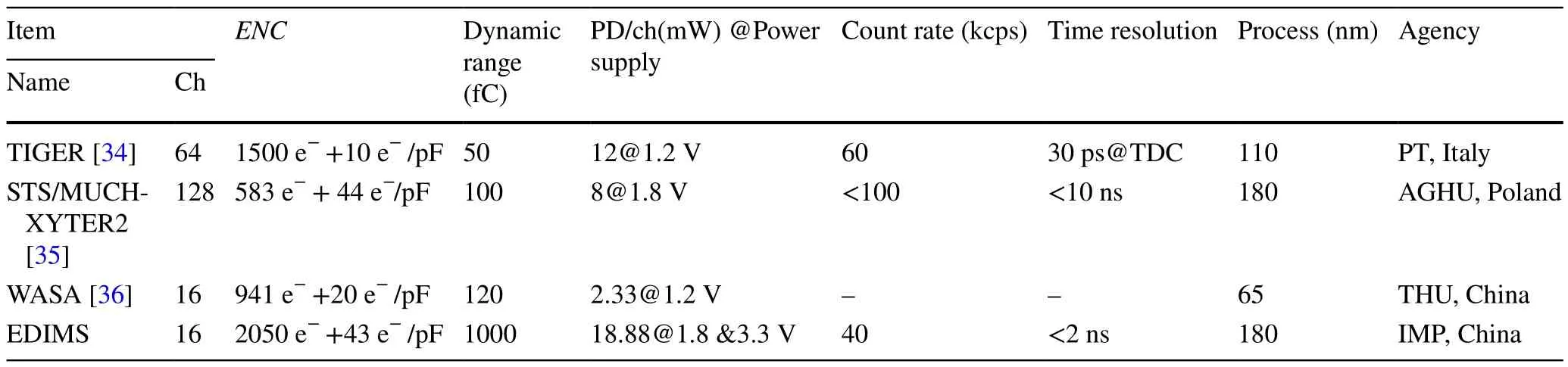
The time resolution of the timing leading edge is determined by the time error of the leading edge and time interval measurement resolution.The time error of the trigger leading edge is mainly composed of the time jitter and walk time.In the case of a fast shaper with a specific shaping time, the time jitter (σ) is determined by the comparator input noise and threshold value [23].Simulations show that the time jitter (σ) of the comparator output signal is 6.46 ps(measured at a reasonable threshold).Therefore, considering that the primary source of time error corresponds to the time walk, TWC is proposed for use in the circuit.The output signals of the fast shaper are fed into comparators a and b, which are compared to the threshold values Vth1 and Vth2 (Vth1 A 4-bit current-steering DAC [24] is designed to provide a configurable difference between Vth1 and Vth2 in response to the need for time-walk compensation at different threshold selections.Cascode current mirrors are used to improve the accuracy of DAC.Simultaneously, a high-gain OPA is used for current–voltage conversion to reduce the effect of the offset voltage. 3.4.2 Timestamp The EDIMS internal time interval measurement module uses a 128-MHz main clock, thus obtaining a coarse time resolution better than 8 ns.To further improve time resolution,clock multiphase techniques [25, 26] are implemented.The working process of the timing resolution compensation is shown in Fig.3a.Four clock signals with a 90-degree difference in phase difference are fed into the counter.Four clocks sample the trigger signal arriving at any moment to form a 4-bit fine time counter, encoded, as shown in Fig.3b.Therefore, the time resolution, which is previously better than 8 ns, increases to more than 2 ns.The counter restarts counting each time it overflows, causing the overflow signal OV to generate a pulse (128-MHz clock synchronization). To satisfy the requirements of the clock multiphase design, a clock 90-degree phase shift circuit [27] is designed, and its schematic block diagram is shown in Fig.3c.CLK_ IN (from FPGA) inputs a low-pass shaping model consisting of inverters, voltage-controlled resistors,and capacitors.An adjustable phase delay is obtained using voltage-controlled resistors.Furthermore, CLK_ IN is also used as a reference clock for comparison with the invertedclock signal after two 90-degree phase shifts in the phasefrequency detector (PFD).The charge pump (CP) feeds the comparison results back to the control side of the voltagecontrolled resistor, which locks a 90-degree phase shift.The adjustable resistance range of the voltage-controlled resistor determines the range of clock cycles to which the circuit can be adapted.It is also necessary to ensure that the inverter output in the 90-degree shifter module is rail-to-rail.Otherwise, duty cycle problems are introduced.The dead time in the PFD should be minimal to reduce the phase difference between the two input signals of the PFD. Fig.3 (a) Timing diagram of clock multiphase, (b) diagram of timestamp encoding, and(c) schematic diagram of clock 90-degree phase shift circuit The analog memory consists of a pointer controller, 4-bit switched capacitor array, and analog buffer as shown in Fig.4a [28].The bottom plate of the four memory capacitors is grounded, and the top plate of each capacitor is controlled by independent read, write, and clear switches for signal write, readout, and reset.No buffer is inserted into the path from the capacitor readout to SCA_BUS; therefore, the bus reset signal bus _clr is designed.The bus is reset when no signal is read.The timing of SCA is shown in Fig.4b.When an internal trigger is generated, the monostable circuit generates a corresponding pulse to drive the W _CTL signal of the pointer to turn on one of the four write switches (one hot).Therefore, the analog amplitude of the energy channel PDH hold is written to the SCA after each internal trigger generation.The read pointer of SCA is controlled by a token ring and has the same one-hot design as the write pointer.SCA is designed with “first input, first output” readout logic to maintain synchronization with the FIFO.The charge in one capacitor is cleared when the next capacitor is read.The analog signal synchronized with the digital data is obtained using SCA_BUS. CMOS switches are chosen as write, read, and clear switches, considering the dynamic range of the input signal and charge injection at the moment of switching off.A switch with a dummy is designed to compensate for the charge injection, as shown in Fig.4c, L1=L2=L3=L4,2W2=W1, 2W4=W3.To reduce the impact of clock feedthrough, the MOSFETs in the switch are chosen to be minimal while meeting the on-state resistance requirement.The ratio of the sampling capacitance of the SCA to the input capacitance of the buffer does not affect the signalto-noise ratio (SNR) of the SCA.However, the SCA output signal must pass through the analog-MUX and analog bus buffer, and a larger output signal is beneficial for improving the SNR of the analog bus buffer output.The large sampling capacitance also aids in improving the matching and obtaining a low KT/C noise while reducing the impact of charge injection into the writing switch.Therefore, a large sampling capacitance and small buffer input capacitance are designed. The clock-synchronized FIFO is designed to store the timestamp information of the trigger signal.The packet formats are presented in Table 2.FIFO, with a 4-bit depth and24-bit width, is a parallel write (128 MHz) and is divided into four 6-bit packet readouts (128 MHz).The FIFO and SCA are designed to be written and read synchronously to ensure timing stability and data matching. Fig.4 (a) Schematic diagram of SCA, (b) timing diagram of SCA, and (c) schematic of the switch with dummy Table 2 Packet format of FIFO Fig.5 Timing diagram of polling The 32-MHz (128-MHz main clock frequency division)token ring [29] is designed for clock-synchronous readout.The polling timing is shown in Fig.5.When there is a channel FIFO transition from empty to nonempty, the ||Empty signal is delayed by 160 ns and then decreases.This causes the token to access each channel, starting from the first channel.The polling and empty signals of the currently accessed FIFO channel operate logically to generate the polling signal.If the current access channel FIFO is empty, then the data are not read, and the token remains for one polling cycle.If it is not empty, then the data in the FIFO and SCA are read to the digital and analog buses.When there are no data to read, the digital bus will hold the last data, and the analog bus will slowly drain to the baseline level starting from the last data.Therefore, a valid signal is designed to mark data validity.It is set synchronously when valid data are read.A valid signal is also used as the synchronization signal required for external data acquisition. When considering EDIMS with 64 channels (the future target), the period to traverse all channels is 2μs.The write rates of the FIFO and SCA match the read rate when the count rate is 500 kcps.The EDIMS storage depth is 4-bit.Hence, the peak count rate of nuclear events that can be satisfied by the storage and token ring is 2 Mcps wherein a maximum of more than five events are allowed for recording in 2μs.A full judgment and drop mechanism is not designed in the SCA; therefore, the SCA continues to write PDH data to overwrite the earliest stored signals in the current SCA when it overflows.The FIFO drops new data when it overflows.Therefore, a switch in the front-end path is designed.When the FIFO in the channel is judged to be full, the frontend path is disconnected to ensure the matching of analog and digital data.For sparse and random detector signals, the pileup of the CSA does not affect the resolution of the time and energy of the fast and slow shaping circuits (when the CSA is not outside the operating region).Monostable and PDH enable front-end dead times of less than 1μs , matching count rates from 500 kcps to 2 Mcps.In this 16-channel prototype chip, the main clock is still used at 128 MHz to satisfy the timing resolution requirements.Therefore, the token ring maintained a polling frequency of 32 MHz, and the period required to traverse all channels is 500 ns. The layout of the EDIMS 16-channel prototype chip is shown in Fig.6a.The dimensions of the die are 3 mm ×3 mm.To ensure the timing stability of digital circuits, crucial digital modules, including the FIFO, Token Manager,and time interval measurement modules, are integrated into one module.The module placed on the right side of the layout is based on the design of a fully customized digital process for the standard library.The left side of the layout shows a 16-channel analog circuit that includes the comparators and SCAs.The bias channel is located in the middle of the 16 channels.Some key signals in channel one are monitored using a buffer.The remaining PADs are used for Qin.The upper and lower PADs provide multiple power, ground,bias, and reference voltages.The right PADs are used for clock input and monitoring, digital resetting, and analog and digital bus outputs. To reduce the interference of digital signals with the analog front end, digital circuits are placed far away from the analog circuits in the layout.The dual-guard ring [30]isolates the digital module from noise sources.The inner ring is connected to the highest independent potential NWELL, and the outer ring is connected to the lowest independent potential PPLUS.A wide strip of PPLUS,connected to the lowest independent potential, is placed between the digital and analog parts.PPLUS strengthens the substrate contact and provides a drain path for noise currents on the substrate, thereby stabilizing the nearby substrate potential.The shielding and protection layout are shown in Fig.6b.The digital IOs are independently powered and disconnected from the analog IOs to avoid the impact of current spikes from the digital IOs to the analog IOs.In analog circuits, all MOS are protected by the majority of carrier protection rings.The modules with high dynamic currents, such as the CSA, comparator, analog_buffer, and test_buffer, are also powered independently.Furthermore, some decoupling capacitors and multilayer power supplies are also designed inside the EDIMS to reduce the power supply noise and voltage drop. To evaluate the performance of the chip, EDIMS is tested in the laboratory using a signal generator (Agilent 81150A)[31], oscilloscopes (Lacroy HDO 4054 [32] & Tektronix 5 Series [33]), and FPGA development board (XILINX K7). The test bench and site diagrams are shown in Fig.7a and b, respectively. 4.1.1 Baseline noise In the self-triggered no-input operation mode, the baseline level and noise are measured at 1.965 V (mean) and 1.28 mV(σ), respectively.As EDIMS contains no analog bus reset logic, the analog bus builds itself up to a level near 2 V.This baseline lift occurs because the analog-MUX input node is highly resistive when there is no trigger, and the bus buffer feeds the charge to raise the level at this point.However,owing to the strong drive of the SCA output, the analog bus is driven to the correct potential by the SCA when a self-trigger is generated.This phenomenon does not affect the proper operation of EDIMS in the self-triggering mode.In the external trigger mode, the baseline level and noise of the fixed channel are measured as 1.355 V (mean) and 2.59 mV (σ), respectively. Fig.7 (Color online) (a) Block diagram of the test bench and (b) diagram of the test site 4.1.2 Channel consistency and time resolution of self-triggering The EDIMS output time information contains timestamps and timer overflow bits (OV).Therefore, trigger consistency and time resolution are measured directly via the timestamps.Prior to this, the digital circuitry sections for timestamp writes and polled reads are verified for reliability via external triggering with 100% digital multichannel consistency.Channel 12 is not included in the analysis of the time and energy characteristics in Sect.4.1.3 owing to an internal trigger anomaly. For trigger time consistency measurements, the signal source feeds the charge signal (500 fC) into the 16 channels of the EDIMS synchronously via a 16-channel charge converter board.Data on the digital bus are acquired, including the channel number, timestamp, and parity bits.The parity bits are first checked to ensure data validity.The overflow bit(OV) is configured for the FPGA to add bits to the counter to avoid interference with data processing due to EDIMS counter overflow, ensuring that it does not overflow in a single experiment.In the data processing phase, the time difference between each channel and reference channel for every trigger is calculated.A Gaussian distribution fit is then applied to over 1000 valid events, resulting in Fig.8a.This figure displays the consistency of the results for 16 channels in comparison with channel 1.The average time difference is under 5 ns, with a time resolution sigma of approximately 1 ns. The test bench for the time-resolved measurements is the same as that for the consistency measurements.The time between each pair of adjacent channel triggers is measured during data processing.A Gaussian distribution fit is performed over more than 1000 effective times, and the resulting sigma is considered as the time resolution of each channel.Sixteen channels are sequenced, and Fig.8b is obtained.Figure 8b shows that the time resolution (σ) for each of the 16 channels ranges between 0.9 and 1.6 ns. 4.1.3 Linearity and energy resolution During the energy test, a single-channel charge adapter plate is used to input a 30-1000-fC charge signal into one channel.For each input charge, the data on the analog bus,synchronized with the valid signal, are acquired using an oscilloscope.Analog bus valid data, collected over 1000 times, serve as a Gaussian distribution fit.The mean value acts as an indicator of the linearity of the slow path,which includes the CSA, slow shaper, PDH, and SCA, as depicted in Fig.9a.The sigma value serves as the outcome of the energy resolution measurement, showcased in Fig.9b.Figure 9b reveals that the energy resolution exceeds 1% (forQin>400 fC), while the poorest energy resolution (σ), measured at 30 fC, is 4.42%.The data in Fig.9a undergo analysis to yield results on baseline and gain inconsistency, as characterized in Fig.9c.The integral nonlinearity per channel appears in Fig.9d.Furthermore, Fig.9c displays a peak baseline error of 78.24 mV, with 75% of the baseline spanning between 1.355 and 1.385 V.Furthermore, the conversion gain range lies between 0.778 mV/fC and 0.802 mV/fC (excluding channel 11).Figure 9d indicates that the INL surpasses 0.5%(bar 11 channels) over an input dynamic range of 30–1000 fC.Variability in the fast shaper baseline and noise effects makes certain channels prone to false triggers, leading to the writing of invalid data to the analog bus at low thresholds.Hence, linearity and energy resolution assessments for signals below 30 fC face limitations due to the false trigger rate hence go unmeasured. The output of the SCA in the test channel is routed offthe chip through a separate analog subline.The energy resolution measurement on this subline is not affected by false triggers in other channels.An energy resolution (σ)of less than 30 fC is measured in this channel at 18.8%(measured at 10 fC). 4.1.4 Counting rate test The decay time of CSA in the test channel is measured.The results show that the CSA has a 97.3% decay rate at 20μs , 96% decay rate at 15μs , and 91.7% decay rate at 10μs(decay rate = decayed signal amplitude/peak signal amplitude).In the test with a count rate of 40 kHz, the EDIMS time and energy resolution exhibit no significant changes,and no pileup occurs in CSAs. This paper presents the design and test results of EDIMS and a 16-channel front-end readout chip for HFRS-TPC.EDIMS features an event-driven, internal memory, and clock-synchronous readout architecture, which is designed to realize high count rates and high integration levels for time and energy measurements.The test results show that the signal chain of the first EDIMS prototype chip functioned correctly.The performance of the chip is as follows:dynamic range of 30–1000 fC, INL of energy measurement exceeds 0.5% (except for 11 and 12 channels), time resolution (σ) ranges from 0.9 to -1.6 ns, the energy resolution (σ)exceeds 1% (Qin>400 fC), and the worst energy resolution(σ) (measured at 30 fC) is 4.42%, which essentially satisfies the requirements. Fig.9 (a) Diagram of the slow path linearity, (b) diagram of energy resolution, (c) diagram of baseline and gain inconsistency, and (d) diagram of channel integration nonlinear inconsistency Table 3 Comparison of EDIMS and other ASIC chips for TPC applications Table 3 shows the comparison between EDIMS and other ASIC chips for TPC applications.EDIMS provides a large dynamic range and a small time resolution with reasonable power consumption and noise levels.The storage mechanism of EDIMS in data transmission has advantages in signal de-randomization and de-sparsification, which are conducive to improving the count rate in the future. Baseline inconsistency and noise will be optimized in the next version, whereas the CSA will be optimized to further improve count rates, making it more suitable for future engineering applications. Author contributions All authors contributed to the study conception and design.Material preparation, data collection, and analysis were performed by Ming-Yu Yang, Yi Qian, Tian-Lei Pu, Wei-Jian Lu, Zhi-Kun Sun, Hong-Yun Zhao, Jia-Rui Zhang, and Zheng-Qiang Liu.The first draft of the manuscript was written by Ming-Yu Yang, and all authors commented on the previous versions of the manuscript.All authors read and approved the final manuscript. Data availability The data that support the findings of this study are openly available in Science Data Bank at https://doi.org/10.57760/sciencedb.j00186.00316 and https://cstr.cn/31253.11.sciencedb.j00186.00316. Declarations Conflict of interest The authors declare that they have no competing interests.
3.5 Analog memory and FIFO


3.6 Token ring and polling readout logic

3.7 Layout design
4 Test results of the chip
4.1 Performance test in the laboratory

5 Conclusion and outlook

 Nuclear Science and Techniques2023年12期
- Nuclear Science and Techniques的其它文章
- A machine learning approach to TCAD model calibration for MOSFET
- BL02U1: the relocated macromolecular crystallography beamline at the Shanghai Synchrotron Radiation Facility
- Coin-structured tunable beam shaping assembly design for accelerator-based boron neutron capture therapy for tumors at different depths and sizes
- Simulation study of BESIII with stitched CMOS pixel detector using ACTS
- Advances in nuclear detection and readout techniques
- Enhancing betavoltaic nuclear battery performance with 3D P+PNN+multi-groove structure via carrier evolution