
Enhancing betavoltaic nuclear battery performance with 3D P+PNN+multi-groove structure via carrier evolution
2024-01-10 10:49HouJunHeYunChengHanXiaoYuWangYuMinLiuJiaChenZhangLeiRenMingJieZheng
Nuclear Science and Techniques 2023年12期
Hou-Jun He · Yun-Cheng Han · Xiao-Yu Wang,4 · Yu-Min Liu · Jia-Chen Zhang,2 · Lei Ren,2 ·Ming-Jie Zheng
Abstract Betavoltaic nuclear batteries offer a promising alternative energy source that harnesses the power of beta particles emitted by radioisotopes.To satisfy the power demands of microelectromechanical systems (MEMS), 3D structures have been proposed as a potential solution.Accordingly, this paper introduces a novel 3D 63Ni–SiC-based P+PNN+ structure with a multi-groove design, avoiding the need for PN junctions on the inner surface, and thus reducing leakage current and power losses.Monte Carlo simulations were performed considering the fully coupled physical model to extend the electron–hole pair generation rate to a 3D structure, enabling the efficient design and development of betavoltaic batteries with complex 3D structures.As a result, the proposed model produces the significantly higher maximum output power density of 19.74 μW/cm2 and corresponding short-circuit current, open-circuit voltage, and conversion efficiency of 8.57 μA/cm2, 2.45 V, and 4.58%, respectively, compared with conventional planar batteries.From analysis of the carrier transport and collection characteristics using the COMSOL Multiphysics code, we provide deep insights regarding power increase, and elucidate the discrepancies between the ideal and simulated performances of betavoltaic batteries.Our work offers a promising approach for the design and optimization of high-output betavoltaic nuclear batteries with a unique 3D design, and serves as a valuable reference for future device fabrication.
Keywords Betavoltaic nuclear battery · High-output power density · Three-dimensional structure · Carrier drift–diffusion ·Carrier recombination · Carrier collection efficiency
1 Introduction
With remarkable performance, compact size, and high-volume production, microelectromechanical systems (MEMS)have attracted tremendous interest for various applications ranging from mobile electronics to deep-sea surveys,implantable medical devices, and autonomous wireless sensor networks.However, the development of micro-batteries capable of outputting power of 1–100 μW, long service life,and fitting within the size range of 1 μm–10 mm has become a critical challenge for MEMS applications [1–3].Recently,betavoltaic nuclear batteries have emerged as a highly attractive energy option for MEMS applications, with the potential advantages of long operational life, high energy density,ultra-miniature size, and strong anti-interference [4–7].
The performance of betavoltaic nuclear batteries is governed by radioisotope source characteristics, device geometry, and semiconductor converter properties.The corresponding relationship can be mathematically expressed as:
whereAis radioisotope activity determined by the radioisotope half-life,Eavgis the average β-decay energy dictating the total input power driving the converter,ηsis the fraction of β-energy emitted to the total decay energy of the radioisotope source,ris the reflectivity coefficient,ηcis the energy conversion efficiency of the semiconductor converter,Qis the carrier collection efficiency,VOCis the open-circuit voltage,FFis the fill factor, andεis the effective ionization energy to generate an electron–hole pair (EHP).The overall conversion efficiency can be expressed as:ηtot=ηs(1 -r)ηc.The output power of betavoltaic nuclear batteries depends on significant losses, such as self-absorption loss (1 -ηs) in the radioisotope source, backscattering loss (r) at the semiconductor interface, and carrier collection loss (1 -Q) outside the depletion region [8–10].To maximize the energy coupling between the radioisotope and semiconductor, it is crucial to increase their face-to-face area while reducing self-absorption and backscattering effects.Additionally,ηcdepends on the material properties of the semiconductor,including bandgap, depletion region width, and carrier diffusion length.Q,VOC, andFFcan be improved via optimization of doping concentrations and junction width to increase the depletion region width and carrier diffusion length,ensuring that the β-particle penetration depth matches the converter scale length.
As the conventional planar configuration of betavoltaic nuclear batteries uses only one side of the radioisotope source attached to the semiconductor converter, the output power and conversion efficiency are limited.A high activity(A) or input power (Pin) requires a thick source layer, but this results in stronger self-absorption effects and smallerηs, saturatingA·ηs.The directional loss is approximately 50%, and the backscattered loss significantly reduces the device efficiency by up to 25% [10, 11].Although efforts have been made to improve the conversion efficiency and output power of betavoltaic nuclear batteries, including use of a reflector to reduce directional loss and backscattered loss [12], optimization of the junction depth and doping concentration to increase the carrier collection efficiency[13–16], use of an extra graded N layer to reduce radiationinduced EHPs recombination loss [17], and adoption of radioisotope sources with higher particle energy to increase input power [18]; their reported values remain limited by the effective loading activity of the radioisotope source as well as the coupling efficiency between the source and device,i.e., the limitation ofAηs(1 -r).As a result, the respective output power is only 0.1–50 nW for practical and tested batteries [18–22] and 10–400 nW for theoretically predicted ones [13–15, 19, 23, 24], falling short of meeting the power requirements of MEMS [25].
To achieve higher performance in betavoltaic nuclear batteries,Aηs(1-r) can be increased over a wide range using specific types of radioisotope sources and semiconductor materials.Increasing the specific surface area of the converter can enable a higher loading amount of radioisotope sources,leading to largerAηs(1 -r) and higher output power.Compared with two-dimensional (2D) planar structures, threedimensional (3D) structures with a larger specific surface area can significantly increase the output power density owing to three factors: (i) more radioisotope sources can fill the interspace of 3D structures, (ii) the thinning of radioisotope sources in 3D structures significantly reduces the self-absorption effects, and (iii) the combination of a radioisotope source with 3D structures leads to the interaction of beta particles with the converter in all directions, increasing the collection efficiency of the beta particles.
In recent years, the use of 3D structures in betavoltaic nuclear batteries has demonstrated significant potential for improving the corresponding specific surface area and conversion efficiency; thus, they are promising options for meeting MEMS power demands [26–29].However, conventional 3D structures require preparation of PN or PIN junctions on the inner surface of the microstructure, which significantly affects the leakage current and output performance [28].This is a predominant reason why the device performance is far from ideal, even up to several orders of magnitude, so full use of the 3D structure is challenging.Moreover, while Monte Carlo simulations [15, 30] and empirical formulas[31, 32] are widely employed to calculate the distribution of the EHP generation rate [G(x)] in betavoltaic nuclear batteries with 2D diode structures, the EHP generation rate is rarely evaluated in 3D structured converters combined with radioisotope sources distributed in 3D space.Most currently available models forG(x) in 3D structured converters only describe specific structures with fixed source and device geometries, and cannot accurately evaluate the EHP distribution in 3D structures, highlighting the need for a precise model to advance the development of 3D batteries.
This paper introduces a novel approach that addresses these issues, utilizing a63Ni-SiC-based (P+PNN+) structure with a multi-groove design, enabling the epitaxial growth of graded P and N layers on the substrate without the need of preparing PN junctions on the inner surface of the microstructure.This approach has the potential to significantly reduce leakage current and power losses, thereby narrowing the gap between theoretical predictions and experimental results.In addition, a novel formulaic model is proposed for calculating the complex EHP generation rate in 3D-structured betavoltaic nuclear batteries.The model considers the intricate 3D structure of the converter and radioisotope source, enabling accurate evaluation of the EHP distribution in all possible 3D structures resulting from changes in their geometries.Our fully coupled model, combined with the COMSOL Multiphysics code, involves the entire physical process of carrier evolution, including β-particle generation,energy deposition, radiation-carrier generation, drift–diffusion, and recombination.This study provides valuable insight into the internal mechanisms of carrier transport, collection characteristics, and power increase.From the results,our approach demonstrates maximized output power density with optimized source thickness, converter geometry, doping concentration, and width of each region, outperforming conventional planar batteries.Our novelG(x) model provides a critical tool for designing and optimizing 3D structured betavoltaic nuclear batteries, with potential applications in other betavoltaic nuclear batteries.
2 Model and method
2.1 Device structure
Figure 1a depicts a63Ni–SiC-based betavoltaic nuclear battery with a multi-groove structure, characterized by the ridge width [d], ridge spacing [t], and groove depth[H_source].The converter comprises four layers: a P+-SiC layer, graded P-SiC layer, graded N-SiC layer, and N+-SiC layer, with thicknesses ofH_P+,H_P,H_N,H_N+(the N+-layer thickness is slightly larger than that ofH_N+),respectively.The63Ni source was filled in multi-grooves,surrounded by converters at the sides and bottom (front and rear sides not shown), and enclosed by a metal electrode at the top.This design reduces the directional and electrode shielding losses compared with conventional planar diode structures.The rectangular top section of the device has the area of 1 cm × 1 cm.To prevent PN junction shorting and metal–semiconductor contact formation,techniques such as nitride passivation, plasma-enhanced chemical vapor deposition, and atomic layer deposition can be employed to grow a thin insulating layer (e.g.,Si3N4, SiO2, and Al2O3) with a thickness of 10–100 nm[33–36].This layer effectively blocks the flow of electrons or holes, achieving insulation between the source and semiconductor devices, while having a negligible impact on the energy deposition of the source decay energy in the device.
To ensure good Ohmic contact, the doping concentrations of heavily doped P+-SiC and N+-SiC layers are 1019and 1018cm-3, respectively.The P- and N-SiC layers serve as the core regions of the betavoltaic nuclear battery, generating an internal electric field [→EI] to separate the radiation-induced EHPs.These layers are lightly doped to obtain larger depletion region width [Wd] and minority diffusion length [LnorLp], and promote EHP collection, as depicted in Fig.1b.The gradient interface between the P+/P and N/N+layers generate an extra electric field [→EPand →EN], which reduces battery surface recombination and enhances EHP collection.In this 3D structure, EHPs are mainly generated in the ridges, and hence these areas contribute the most to the output power.Monte Carlo simulations and COMSOL Multiphysics were used to optimize the structural parameters, including the thickness of each doping region, doping concentration, ridge width, and ridge spacing, and predict the battery output performance.
63Ni source was selected as the beta source due to its long half-life (approximately 100 years), moderate decay energy(Eavg= 17.4 keV,Emax= 66.9 keV), and solid metal form,which allows easier and safer handling.SiC was selected as the converter semiconductor material because of its desirable properties including low leakage current density,higher radiation damage threshold, higher conversion effi-ciency, and excellent tolerance to harsh environments, i.e.,extreme temperatures, wear, chemical exposure, and radiation [37–39].Moreover, the development of SiC etching technology has enabled the fabrication of microgroove structures with high aspect ratio [39].
2.2 Methods
2.2.1 Radiation-induced carrier generation in 3D diode structures
2.2.1.1 Model for radiation-induced carrier generation rate in 3D diode structures The distribution of the EHP generation rate in a betavoltaic nuclear battery is governed by the energy deposition of beta particles in the converter, which significantly affects the output performance.In the conventional planar diode structure depicted in Fig.2b, the energy deposition [Edep(x)] along the radiation transport depth [x] in bulk SiC was calculated via a Monte Carlo simulation with the Geant4 radiation transport toolkit, using a rectangular63Ni source with a full energy spectrum.The63Ni source is characterized by the specific activity of 5.68 Ci/g, 100%abundance, and density of 8.9 g/cm3, with isotropic emission of beta particles.SiC has the bandgap width of 3.26 eV,relative dielectric constant of 9.7, density of 3.21 g/cm3, and intrinsic carrier concentration of 7.4 × 10⁻⁹cm-3, derived using the widely employed formula [40].G(x) is obtained and expressed as:
whereAis the activity of the radioisotope,εis the average energy needed to generate an EHP, commonly considered as 6.88 eV for SiC [41], andG0andαare the surface EHP generation rate and absorption coefficient, respectively.G(x)of63Ni sources with varying thickness [t] is presented in Fig.2c, and the correspondingG0andαare derived by fittingG(x).The dependences ofG0andαon the source thickness[t] are then fitted, as demonstrated in Fig.2d.Consequently,G(x) considering different source thicknesses is expressed as:G(x,t)=A1(1-e-μ1t)e-(A2e-μ2t+B2)x, the fitting parameters for which are provided in Table 1.Figure 2c shows that the saturation thickness of the63Ni source is 3 μm, consistent with previous work [24, 42].The penetration depth of β particles emitted from63Ni is 10.2 μm in SiC, defined as the location where 99% of the total energy deposition occurs according to Alam [8].

Fig.2 (Color online) Schematics of a 3D and b 2D converters; c EHP generation rates along penetration depth and d surface EHP generation rate and absorption coefficient for different source thicknesses in 2D converters; EHP generation rates in 3D converter with e 1.5 μm ridge spacing and 3 μm ridge width, f 1 μm ridge spacing and 3 μm ridge width, g 1 μm ridge spacing and 4 μm ridge width
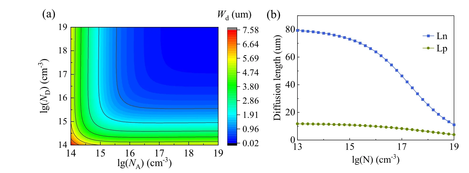
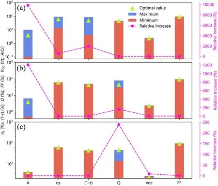
To accurately model the energy deposition and EHP generation rate in a multi-groove betavoltaic nuclear battery, it is essential to consider the superposition contributions of all the isotope sources and ridges.This involves extendingG(x,t) of the 2D structure to that of the 3D structure.Figure 2a characterizes the penetration distance distribution of β particles released by63Ni isotope sources, where Djdenotes thejth layer converter (thejth ridge of the proposed battery) and Sjindicates thejth63Ni layer.At a random location of the EHPs generated in converter Dj(specified by reference site P), the distance between P and source Sj-1is represented by [x].Converter Djis exposed to [j-1] layers of isotope sources on its left, and the β particles emitted from theith (i wherenis the layers of sources,G0(t) is the surface EHP generation rate,α(t) is the absorption coefficient of β-electron flux in SiC, andγ(t) is the absorption coefficient of β-electron flux in63Ni, which are acquired via the equation in Table 1 based on Monte Carlo code simulation.The EHP generation rate of the (n+ 1)th converter can be expressed asGn+1(x,t)=G1(d-x,t) , owing to the symmetry of the multi-groove structure.Table 1 shows that theR2(R-squared or coefficient of determination) values are greater than 0.99, indicating the excellent fitting performance of the model. 2.2.1.2 Validation of electron–hole pair (EHP) generation rate model in 3D diode structures Accurate prediction of the rate of EHP generation is essential for optimizing the design of 3D SiC-based betavoltaic nuclear batteries.Therefore, the validity and ability of the model to predict data from 3D multi-groove structures was demonstrated through comparison with original Geant4 data [AEdep(x)/ε].Figure 2e–g exhibit the reliability of the proposed EHP generation rate model, expressed by formula (3), with highly consistentG(x,t) curves compared with the original Geant4 data for both ridge spacings of 1.5 and 1 μm, and ridge widths of 3 and 4 μm.The highR2values of 0.985, 0.990, and 0.982 for these curves indicate the accuracy of the model in calculating the EHP generation rates in 3D structures, rendering it a valuable tool for optimizing SiC-based betavoltaic nuclear batteries for high performance. In the 2D converter, the EHP generation rate decreased exponentially with depth; whereas, the multi-groove 3D structure exhibits a unique distribution of higher EHP generation rates in the inner ridges and lower rates in the outermost ridges.The innermost ridges exhibit high EHP generation rates on the lateral surfaces, low rates in the middle, and a symmetrical distribution, matching the 3D EHP distribution in the inner ridge shown in Fig.1a.These findings suggest that the proposed multi-groove 3D structure has the potential to significantly enhance the power output compared with the traditional 2D structure, particularly as the relative depth increases. 2.2.2 Model for radiation-induced current in 3D diode structures Figure 1b illustrates that radiation-induced EHPs generated within the depletion region can be collected with 100%efficiency, whereas those generated outside the depletion region can only be collected after diffusion to the PN junction boundary, the P+/P interface, or the N/N+interface.TheCE(y) was calculated using the equation [43]: whered(y) represents the distance from the depletion region boundary or the interfaces and is set to zero inside the depletion region.The electron and hole minority carrier diffusionlengthsLare expressed asLn1,Ln,Lp, andLp1in regions P+,P, N, and N+, respectively.The radiation-induced current densityJRcan be expressed as: Table 1 Exponential fitting parameters and R-squared values for G0(t), α(t), and γ(t) whereqis the electron charge;H1is the ridge width [d]; andH2andSare the rectangular side length (1 cm) and area of the device (1 cm2), respectively. According to the drift–diffusion theory, nonequilibrium carriers generated within the depletion region and the neutral region outside the depletion region boundary within a minority diffusion length can be collected, thus contributing to the current density (JR).The effective charge collection region (ECR) length, represented byH_ECR = (Wd+Ln1+2Ln+ 2Lp+Lp1), determinesJRand can be maximized by increasingWd,Ln1,Ln,Lp, andLp1.Lower doping concentrations increaseWdandL, leading to higher EHP collection, as demonstrated in Fig.3a, b, whereWddecreases from 7.58 μm to 30 nm andLndecreases rapidly from 77.34 to 11.06 μm with increasing doping concentration from 1014to 1019cm-3.Lpdecreases more gradually over the same doping range.The minimum doping concentration in the P- and N-regions was 1014cm-3due to our facility’s capacity to process low doping in SiC materials; whereas, the minimum doping concentration of the heavily doped P+-and N+-regions requiredNA= 1019cm-3andND= 1018cm-3,respectively, to reduce the ohmic contact.To maximizeH_ECR andJR, the maximum values ofWd,Ln1,Ln,Lp, andLp1should be adopted, as listed in Table 2 and detailed in Supplementary Materials S1 and S2. 2.2.3 Battery output characteristic model and simulation The electron (hole) concentration [n(p)] inside the semiconductor converter device is governed by the carrier continuity equation as follows: wherejn(jp) is the electron (hole) current density,Gis the EHP generation rate derived from Eq.(3), andRn(Rp) is the electron (hole) recombination rate.jn(jp) can be described by the drift and diffusion processes [44] as: whereEis the sum of the external and internal electric fields generated by the diffusion of EHPs.These relationships are governed by the Poisson equation:whereρis the charge density,?0is the vacuum permittivity,?ris the relative permittivity of the semiconductor, andND(NA) is the concentration of donor (acceptor). Table 2 Maximum depletion region and minority carrier diffusion length in each region of the converter Fig.3 a Depletion region width and b minority diffusion length with doping concentration 2.2.3.1 Current–voltage characteristics of ideal PN junction diodes The current–voltage (J–V) characteristics of an ideal long PN junction diode can be derived assuming that the external voltage drops entirely in the depletion region, the diode operates under a low injection level (i.e.,the excess carrier concentration is much smaller than the equilibrium majority carrier concentration), there is no recombination or generation current in the space-charge region, the semiconductor is nondegenerate, and the length of the P- (N-) region is much larger than the diffusion length[45, 46]. Under these assumptions, theJ–Vrelationship of the neutral areas (E= 0) of the P- and N-regions can be obtained by solving the continuity Eqs.(6–7) and current Eqs.(8–9).Ignoring the recombination and generation currents in the space-charge region, theJ–Vcharacteristics of an ideal diode are given by: whereJSCis the short current, equals to radiation-induced currentJR;kis Boltzmann’s constant;Tis the absolute temperature (300 K in this work);Vis the bias voltage; andJ0is the leakage current density of the PN junction. The open-circuit voltage is derived asJ= 0 A. Then, the maximum output powerPmcan be described as: whereFFis the fill factor, which can be derived using the open-circuit voltage [13].J0is determined by the diffusion efficiency and diffusion length of the minority carriers, and the doping concentrations, shown in S3 of the Supplementary Materials.Using this ideal diode model, the battery performance can be predicted quickly, and the optimal battery structure can be determined based on the J–V characteristic numerical model. 2.2.3.2 Current–voltage characteristics calculation using COMSOL Multiphysics TheJ-Vcharacteristics of real diodes differ from those of ideal diodes owing to the various assumptions made for ideal PN junction diodes.Therefore, an accurate method is essential to simulate theJ–Vcharacteristics of real diodes, considering the generation, recombination, and drift of charge carriers, as well as the real characteristics of the semiconductor material. COMSOL Multiphysics is a powerful tool for simulating the current–voltage characteristics of realistic situations by solving partial differential equations that incorporate real physical phenomena.The simulation utilizes various physical models, including the Monte Carlo simulation for calculating the EHP generation rate in 3D diode structures (Eq.3), the Shockley–Read–Hall model for trap-assisted recombination(Eq.14) [45], and the low-field mobility model for determining the minority carrier mobility (Eqs.S4–S5 in the Supplementary Materials).Additionally, the carrier lifetime model is described in Eqs.S6–S7 in the Supplementary Materials. hereCn(Cp) is the electron (hole) capture coefficient,niis the intrinsic carrier concentration,τn(τp) is the electron(hole) minority lifetime given by Eqs.S6–S7 of the Supplementary Material,Etis the recombination center (defect)level, andEiis the intrinsic Fermi level.The defect energy level is set asEt=Ei, and the defect density is Solving partial differential Eqs.(6–10), we obtained important information on the electric field, carrier recombination,and electron (hole) current density, enabling prediction of crucial electrical parameters, including the short-circuit current [JSC], open-circuit voltage [VOC], and output power [Pm].Ultimately, with this approach, the behavior of diodes can be accurately modeled, which is vital for optimizing their performance and ensuring that they meet the requirements of various real-world applications. Fig.4 (Color online) Effects of the ridge spacing [t] and ridge width[d] on the a JSC, b VOC, c Pm; the dependences of d Pm, Pin, e d,and ηtot on t. Na and Nd are both set to 1 × 1014 cm-3; H_P and H_N are set to 158 μm and 26 μm, respectively, approximately equal to(2Ln_max + Wd_max/2) and (2Lp_max + Wd_max/2) To optimize the structure of the proposed battery and maximize its output power density, a parametric sweep was conducted in the numerical model to adjust variables including the single-source thickness (ridge spacing,t);single-converter thickness (ridge width,d); thicknesses of the P+-, P-, N-, and N+-regions (H_P+,H_P,H_N, andH_N+); acceptor concentration of P-region (Na); and donor concentration of N-region (Nd).Possible values oftanddare in the range of 0.1–10 μm with a 0.1 μm step size for each.It is worth noting that the source thickness is fixed to the saturation thickness of 3 μm astis greater than 6 μm, and evenly distributed on the inner surface of the microgroove.The feasible ranges forH_PandH_Nare 1–250 μm and 1–60 μm, respectively, whileNaandNdcan range from 1 × 10¹⁴to 7.94 × 1018cm-3and 1 × 10¹⁴to 7.94 × 1017cm-3, respectively.The values forH_P+andH_N+correspond to 10 and 6 μm, which are close to the minority carrier diffusion length in the P+-region and N+-region.Additionally, the heavily doped P+-region and N+-region are assigned acceptor concentration and donor concentration values of 1 × 10¹⁹and 1 × 1018cm-3,respectively. 3.1.1 Optimizing ridge spacing and width The output power of a betavoltaic nuclear battery depends on the amount of beta particle energy deposited in the converters and the efficient collection of radiation-induced EHPs.The coupling between the radiation source and the device is crucial for enhancing the output power.To illustrate the impacts oftanddon the output performance of the betavoltaic battery, the 3D surface contours of the short-circuit current density (JSC), open-circuit voltage (VOC), and maximum output power density (Pm) were plotted, as shown in Fig.4. As depicted in the 3D surface wireframe perpendicular to theddirection in Fig.4a,JSCinitially increases rapidly,but subsequently decreases astincreases, reaching a peak value withtof 0.1–2.2 μm.Additionally, the dependence ofJSCondexhibits a similar trend, reaching its peak withdof 0.2–4.0 μm.The bottom-projected contour shows that the optimal values ofJSCare achieved whendis in the range of 0.2–3 μm andtranges from 0.1 to 2 μm.The maximumJSCof 8.57 μA/cm2is achieved by combiningt= 0.8 μm andd= 1.2 μm. Figure 4b demonstrates thatVOCinitially increases astincreases and reaches saturation att= 2 μm, while it decreases with an increase ind.Nevertheless, overall,VOCis not highly sensitive to variations intandd, with a range of 2.36–2.46 V.Due to the minor variation inVOC,Pmis primarily determined byJSC.The relationship betweenPmand variations intanddexhibit similar trend to that ofJSC, with a rapid initial increase and a subsequent slow decrease with increasingtord, as illustrated in Fig.4c.The maximumPmvalue of 19.73 μW/cm2is attained att= 0.8 μm andd= 1.2 μm. The factors affecting the output power mainly includeA,ηs, (1 -r),Q,VOC, andFF.With varyingtandd,A,ηs,(1 -r),VOC, andFFexhibit relative increases of 9844.28%,578.19%, 1956.94%, 4.14% and 0.21%, respectively, whileQremains unchanged at 45.64%.Therefore, the key factor affecting the output power is the coupling ofA,ηs, andr.For the detailed calculation process, please refer to Supplementary Material S4. The input power [Pin] can be calculated by combiningA,ηs, andr, asPin=AEavgηs(1 -r).Figure 4d–e present the maximum output power [Pm] and its corresponding optimized ridge width [d] of 0.2–4.0 μm, for different source thicknesses [t].We found thatPmis determined by the coupling ofA,ηsandr, i.e.,Pin.The optimized value ofdgradually saturates with increasingt, consistent with the phenomenon of energy deposition saturation in the converter with increasingd.Additionally, the overall conversion efficiency[ηtot] increases and then decreases witht, reaching a saturated value of approximately 1.5%, andηtotcorresponding to maximumPinandPmis 4.58%. In the proposed battery, smaller ridge spacing and ridge width can improve the source activity and reduce the selfabsorption effect.However, excessively thin converters may result in a lower (1 -r) and do not match the particle penetration depth, leading to a reducedPin.Therefore, a tradeoffbetweentanddis necessary to maximize the power density. 3.1.2 Optimizing widths of P-region and N-region After optimizingtandd, we investigated the dependence ofJSC,VOC, andPmon the widths of the P- and N-regions for betavoltaic nuclear batteries, as shown in Fig.4a–c.IncreasingH_P results in an initial increase and subsequent saturation ofJSC,VOC, andPm.This trend can be attributed to the increase in the radioisotope source activity withH_P,which generates more EHPs in the ECR.However, whenH_P exceeds the ECR length, the performance metrics reach saturation.Specifically,JSC,VOC, andPmsaturate whenH_P reaches 160 μm, and an additional increase of 10 μm results in a negligible increase of less than 1%.Similarly,JSC,VOC,andPmpresent a similar trend withH_N, showing a gradual rise and saturation atH_N = 24 μm.This phenomenon can be attributed to the longer minority carrier diffusion length(Ln= 77.34 μm) of the P-region compared with that of the N-region (Lp= 11.44 μm), and their saturation values ofH_P andH_N are around twiceLnandLp, respectively.Therefore,H_source should not exceed 200 μm, whereH_P+andH_N+are 6 and 10 μm, respectively, andH_P andH_N should not exceed their saturation values, corresponding to 160 and 24 μm. Figure 5d shows thatAlinearly increases withH_P from 0.51 to 6.59 Ci (by 1204.00%), whileQfirst increases and then decreases with the relative change rate of 164.92%.The optimization ofH_P reveals that factorAis the dominant factor affecting the output power, and factorQis secondary.AlthoughAandQshow different trends with changes inH_P, their products,A·QandPm, exhibit consistent trends,further confirming thatAandQare the key factors affectingPm, as shown in Fig.5e.However,VOCandFFincrease minimally by 1.81% and 0.09%, whileηsand (1 -r) remain unchanged at 61.53% and 48.77%, respectively.Please refer to Supplementary Material S4 for detailed calculations. As depicted in Fig.5f, for the structure withH_source = 200 μm,JSCandPminitially increase withH_P and then decline instead of continuously increasing.This behavior is due to the contribution ofH_N toJSC, andPmoutweighs that ofH_P whenH_P approaches its saturation thickness.Therefore, when optimizing the widths of the Pand N-regions, the balance betweenH_P andH_N should be considered, as the combination ofH_P = 156 μm andH_N = 28 μm achieves the maximumPmof 19.74 μW/cm2.A longer P-region is more suitable for a betavoltaic nuclear battery with a P+PNN+junction structure because it is more conducive to enhancing the collection of EHPs owing to the larger minority carrier lifetime and mobility compared with the N-region, as shown in Fig.S2 in the Supplementary Material. 3.1.3 Optimizing doping concentration in P- and N-regions Based on the analysis in Sect.2.2.2, the doping concentration plays a crucial role in determining the depletion width and minority carrier diffusion length of the betavoltaic nuclear battery, which significantly affects the collection efficiency of the EHPs and the output performance of the battery. Figures 5c and 6a illustrate the effects ofNaandNdonJSC,VOC, andPmfor the proposed battery.As shown in Fig.6a,JSCincreases with a decrease inNaowing to its beneficial effect of expanding the minority carrier diffusion length and depletion region width to promote EHP collection, as depicted in Fig.3.The variation inJSCwithNdwas small compared withNabecauseLpis much smaller thanLn, resulting in less changes in the collection efficiency of EHPs. Figure 6b shows thatVOCinitially increased rapidly but subsequently decreased slowly asNaincreased, as depicted in the 3D surface wireframe perpendicular to theNddirection.The dependence ofVOConNdexhibits a similar trend.The maximumVOCof 2.66 V is obtained by combiningNa= 3.16 × 1018cm-3andNd= 7.94 × 1017cm-3.The bottom-projected contour indicates that the optimal values ofVOCare achieved at higher doping concentrations, which is attributed to the reduction in the leakage current [J0]owing to the higher doping concentration, as demonstrated in Fig.S3 in Supplementary Material. Fig.5 (Color online) Effects of H_P and H_N on a JSC, b VOC, and c Pm with varying H_source; dependences of d A, Q, e Pm, and A·Q on H_P with H_N fixed at 24 μm; f dependence of Pm on H_P with H_source = 200 μm.Na and Nd are both set to 1 × 1014 cm-3, t = 0.8 μm,and d = 1.2 μm AlthoughJSCandVOCexhibit opposite dependencies on doping concentration,Pmvaries in the same way asJSCbecause the variation range ofVOCwith doping concentration is small, of 2.44–2.66 V with a relative increase of 8.98%.The optimal doping concentration combination isNa= 1 × 1014cm-3andNd= 1 × 1014cm-3, yielding the maximum output power density of 19.74 μW/cm2. As shown in Fig.6d, low doping increasedQfrom 13.48 to 45.65% owing to the widened depletion region and diffusion length, leading to longer ECR length [H_ECR] and improved EHP collection, and resulting in a higher power density.H_ECR andPmfollow a similar trend asQ, confirming that low doping enhances the power density by increasingH_ECR for EHP collection.However, at the highest doping concentration,H_ECR andPmare minimum, of 53 μm and 6.37 μW/cm2, respectively, which are only slightly better than the power of 5.80 μW/cm2with theH_source of 53 μm.Pmonly marginally improves even with a nearly four-fold increase in the source activity [A],indicating the critical role ofH_ECR in the design of the 3D battery and thatH_source should not exceedH_ECR.Additionally,FFranges from 94.18 to 94.57%, with a tiny relative increase of 0.42%, whileA,ηs, and (1 -r)remain constant at 4.04 Ci, 61.53%, and 48.77%, respectively, resulting in constantPinof 129.16 μW/cm2.Therefore,Qis a significant factor affecting the output power density, and a low doping concentration in the P- and N-regions is recommended to enhance it, hence maximizing the short current and output power density.Detailed calculations are provided in Supplementary Material S4. 3.1.4 Critical parameters of device structure To achieve the best device performance, we comprehensively optimized the geometric dimensions (optimization procedure #1), doping concentration (optimization procedure #2), and width of each doping layer (optimization procedure #3) of the semiconductor materials.The final optimized parameters for the battery areNa=Nd= 1 × 1014cm-3,H_P = 156 μm,H_N = 28 μm,t= 0.8 μm, andd= 1.2 μm. Fig.6 (Color online) Influence of Na and Nd on a JSC, b VOC, and c Pm; effect of Na on d H_ECR, Q, and e Pm.H_P = 156 μm, H_N = 28 μm,t = 0.8 μm, and d = 1.2 μm In Optimization procedure #1,A,ηs, and (1 -r) exhibited significant relative increases, while the relative increases inQ,VOC, andFFwere negligible, as shown in Fig.7a.Therefore, the key factor affecting the output power is the coupling ofA,ηs, and (1 -r), and a tradeoffbetween them is required to maximize the power density, as depicted by their optimal parameters corresponding to the maximum output power. In Optimization procedure #2,Awas identified as the dominant factor affecting the output power, with the significant relative increase of 1204.00%, andQwas a secondary factor with the relative increase of 164.92%, as depicted in Fig.7b.IncreasingH_P andH_N can enhance the source activity [A] and ECR length.However, increasingH_P andH_N beyond the ECR leads toQ, as EHPs outside the ECR become difficult to collect.The tradeoffbetweenAincreasing andQdropping results in saturation of the output power. In Optimization procedure #3, we found thatQis the key factor affecting the output power; whereas, the other factors have negligible relative increases, as shown in Fig.7c.To optimize the output power density, low doping concentrations should be used in both P- and N-regions.This enables larger diffusion lengths and wider ECRs, resulting in a higher collection efficiency of EHPs, particularly through an extendedH_ECR. Among these parameters, the coupling ofA,ηs, and (1 -r)has the greatest impact on the output performance, which is related to the activity, self-absorption, and backscattering of the radioactive source.The second most influential parameter isQ, which depends on the depletion region width and diffusion length controlled by the doping concentration,as well as the ECR length governed byH_P,H_N, and the doping concentration.To maximize the output power density, use of thinner sources and converters, lower doping concentrations, and largerH_P, of approximately twice the diffusion length, are recommended. To validate the numerical model established in this study, we performed calculations on planar batteries with the same geometric dimensions and semiconductor parameters as those in references [24] and [16]; good agreement was apparent regarding the output power density, as shown in Table 3.It is worth noting that the power density of battery #1 was converted based on the 100% abundance of63Ni source, in contrast to the 20% abundance mentioned in reference [24].The difference in the results between reference[16] and this study (#5 battery) is relatively large becausethe previous work did not consider the energy loss caused by the collection efficiencyQ, leading to an overestimation ofPm.Using our method, we can further provide suggestions for optimizing the batteries in references [24] and [16] by adjustingNa,Nd,H_P andH_N.For reference [24], settingH_P,H_N,Na, andNdto 4.9 μm, 19.9 μm, 1 × 1014cm-3, and 3.98 × 1014cm-3, respectively, the maximum output power can be increased to 296.5 nW/cm2, representing a 12.6%improvement as depicted by battery #3.For reference [16],by combiningH_P = 0.1 μm,NaandNdat 4.7 × 1013cm-3and 3 × 1016cm-3, respectively, the output power can be increased to 378 nW/cm2, with a 10.5% improvement as depicted by battery #6. Fig.7 (Color online) Optimal parameters and their relative increase considering different optimization procedures: a Optimizing t and d; b Optimizing H_P and H_N; c Optimizing Na and Nd.Relative increase is calculated as the difference between the maximum and minimum values divided by the minimum value.The bars show the minimum values only, indicating that the maximum value is equal to the minimum Fig.8 (Color online) Discrepancies between the ideal and practical performances simulated by COMSOL: a Dependences of Pm, Q,b VOC, and FF on H_P; c Distribution of electric field and carrier recombination rate; d Dependences of (G-R) distribution on H_P and d.(G–R) represents the difference between the generation rate and the recombination rate of EHPs Finally, we conducted a comparative analysis of the P+PNN+and PN structures, assessing their respective output power densities in the 2D (#7 and #8) and 3D (#9 and#10) batteries.To achieve this, we substituted the P+and N+layers in the P+PNN+structure with P and N layers of the same size to obtain the PN structure, as shown in Table 3.Our results indicate that the P+PNN+structure outperforms the PN structure, with a 10% increase inPmin the 2D configuration and a 39% increase in the 3D configuration.These findings highlight the superior performance of the P+PNN+structure, particularly in 3D configurations. In this study, the diffusion lengths were calculated through commonly used equations [17, 42], and the minority carrier lifetimes (τnandτp) adopted in these calculations(shown in Supplementary Material S4) fall within the range of experimental values (τnof 0.9–10 μs andτpof 0.05–2.1 μs) [47–50].Moreover, experimental diffusion lengths for SiC were reported to be 30–100 μm [49, 51], which provides further validation for the calculated electron and hole diffusion lengths presented in this article. The largest discrepancies between the ideal and practical performances of betavoltaic nuclear battery are the collection efficiencyQandVOCFF/ε[10].To better understand the discrepancies between the ideal and practical performance of betavoltaic nuclear batteries, it is necessary to conduct a detailed analysis of the specific differences caused byQ,VOC, andFF, as well as their underlying reasons.COMSOL Multiphysics was employed to simulate the practical performance of betavoltaic batteries.Most SiC material properties were imported from the COMSOL library; some properties that were not available in the library, such as minority carrier mobility and minority carrier lifetime, were manually added based on the literature [17]. In the simulation process, a single converter was modeled with dimensions of 1 μm × 1.2 μm × 200 μm.A usercontrolled mesh of four different sizes (#a, #b, #c, and #d)was defined to improve both the accuracy and computation time, with maximum element sizes of 50, 100, 200, and 500 nm.The minimum element sizes were set to 1/10 of the corresponding maximum element sizes.Although the use of finer mesh sizes resulted in slightly largerPmvalues, the differences are negligible.Specifically,Pmvalues obtained from mesh #a are only 0.064%, 0.121%, and 0.149% higher than those obtained from meshes #b, #c, and #d, respectively.Based on these results, the #d mesh was chosen for computation, with boundary elements set at the maximum element size of 0.1 and minimum element size of 0.02.The maximum element growth rate was set to 1.1 with the curvature factor of 0.25, and the resolution of the narrow regions was specified as 1. Figure 8a displays the relationship betweenPmandH_P obtained through numerical modeling and COMSOL simulations.The variations inPmwithH_P from these two methods are in excellent agreement, reaching their maximum values atH_P of 156 and 164 μm, respectively, with values of 19.74 and 18.69 μW/cm2, differing by only 5.62%.However,there were some differences inPmat lower values ofH_P,which increased asH_P decreased.These differences arise fromQ,VOC, andFF, as shown in Fig.8a, b, respectively.The numerical model relies on empirical formulas (4) and(12) forQandVOC, resulting in a lowerQand higherVOCthan the COMSOL simulation, which calculatesQby subtracting the Shockley-Reed-Hall recombination rate from the EHP generation rate (shown in Fig.8d) and extractingVOCby finding the voltage value when the current is nearly zero.In addition, the numerical model produces a higherFFwith little variation, while the COMSOL simulation calculatesFFby dividingPmbyVOCandJSC, which are sensitive to the distribution ofVOC. In addition,Pminitially increases and then decreases with increasingH_P, reaching a maximum value atH_P of approximately 2Ln.This can be explained by the suppression of carrier recombination owing to the electric field distribution.The electric field distribution intensity and range atH_P = 164 μm are much greater than those atH_P = 4 μm, resulting in a considerably lower carrier recombination rate, leading to a largerQand hence a largerPm, shown in Fig.8c.This indicates that the internal mechanism affecting the power increase is the electric field distribution, which governs the carrier transport and collection characteristics. The results demonstrate that the proposed battery has a significantly improved output performance compared with conventional planar batteries reported in previous studies[13–16, 19, 23, 24], with a maximum output power density approximately 50 times higher.If multiple batteries are stacked to a total thickness of around 10 mm, the proposed battery would provide an output power of approximately 1 mW, which can satisfy the power requirements of MEMS with dimensions less than 10 mm and power consumption of 1–100 μW.We provide further recommendations for designing 3D-groove betavoltaic nuclear batteries regarding 3D etching techniques on SiC, as shown in Table S2 of the Supplementary Material. In summary, this paper presents a novel63Ni-SiC-based P+PNN+3D structure with a multi-groove design that eliminates the need for preparing a PN junction on the inner surface of the microstructure and improves the performance of betavoltaic nuclear batteries.The fully coupled model developed in this study considers various factors, such as β-particle generation, self-absorption, backscattering, energy deposition, as well as radiation-induced carrier generation and drift–diffusion, and thus provides a valuable tool for efficient design and development of betavoltaic nuclear batteries with complex 3D structures.The epitaxially grown graded P/N layer significantly enhancesH_ECR, promoting radioisotope source activity and carrier collection efficiency,producing the maximum output power density of 19.74 μW/cm2, with relatively thin radioisotope sources and converters (t= 0.8 μm andd= 1.2 μm), lightly doped P- and Nregions (Na=Nd= 1014cm-3), and longer P-region widths(H_P = 156 μm).The analysis of carrier transport and collection characteristics using the COMSOL Multiphysics code provides insights into the internal mechanism of the power increase and clarifies the discrepancies between the ideal and simulated performances of betavoltaic nuclear batteries.However, the diffusion length is susceptible to process variations and a short diffusion length may reduce the advantages of the proposed P+PNN+3D structure.In conclusion,the proposed 3D structure with a multi-groove design combined with a fully coupled model and optimization methods presents a promising approach for designing and optimizing high-performance betavoltaic nuclear batteries.It is worth noting that the importance ofH_ECR cannot be overstated by increasing the output power, as it directly affects both radioisotope source loading and charge collection efficiency.Furthermore, the 3D structure proposed herein is expected to be well-suited for narrow-bandgap semiconductor materials with ultralong diffusion lengths. See the supplementary material for details of our calculation procedure and recommendations on the device design of betavoltaic nuclear batteries considering three-dimensional etching techniques on SiC. Supplementary Information The online version contains supplementary material available at https:// doi.org/ 10.1007/ s41365- 023- 01331-y. Author contributions All authors contributed to the study conception and design.Material preparation, data collection and analysis were performed by Hou-Jun He, Yun-Cheng Han, Xiao-Yu Wang, Yu-Min Liu,Jia-Chen Zhang, Lei Ren and Ming-Jie Zheng.The first draft of the manuscript was written by Hou-Jun He and all authors commented on previous versions of the manuscript.All authors read and approved the final manuscript. Data availability The data that support the findings of this study are openly available in Science Data Bank at https:// www.doi.org/ 10.57760/ scien cedb.j00186.00275 and https:// cstr.cn/ 31253.11.scien cedb.j00186.00275. Declarations Conflict of interest The authors declare that they have no competing interests.

3 Results and discussion
3.1 Performance calculated using ideal diode model


3.2 Performance simulation using COMSOL Multiphysics
4 Conclusion
 Nuclear Science and Techniques2023年12期
- Nuclear Science and Techniques的其它文章
- A machine learning approach to TCAD model calibration for MOSFET
- BL02U1: the relocated macromolecular crystallography beamline at the Shanghai Synchrotron Radiation Facility
- Coin-structured tunable beam shaping assembly design for accelerator-based boron neutron capture therapy for tumors at different depths and sizes
- Simulation study of BESIII with stitched CMOS pixel detector using ACTS
- Advances in nuclear detection and readout techniques
- Measurement and simulation of the leakage neutron spectra from Fe spheres bombarded with 14 MeV neutrons