
Latest developments in EUV photoresist evaluation capability at Shanghai Synchrotron Radiation Facility
2024-01-10 10:49ZhenJiangLiChengHangQiBeiNingLiShuMinYangJunZhaoZhiDiLeiShiJieZhuHaoShiLuWangYanQingWuRenZhongTai
Nuclear Science and Techniques 2023年12期
Zhen-Jiang Li · Cheng-Hang Qi · Bei-Ning Li · Shu-Min Yang · Jun Zhao · Zhi-Di Lei · Shi-Jie Zhu ·Hao Shi · Lu Wang · Yan-Qing Wu · Ren-Zhong Tai
Abstract Evaluating the comprehensive characteristics of extreme ultraviolet (EUV) photoresists is crucial for their application in EUV lithography, a key process in modern technology.This paper highlights the capabilities of the Shanghai Synchrotron Radiation Facility (SSRF) 08U1B beamline in advancing this field.Specifically, it demonstrates how this beamline can create fringe patterns with a 15-nm half-pitch on a resist using synchrotron-based EUV lithography.This achievement is vital for evaluating EUV photoresists at the advanced 5-nm node.We provide a detailed introduction to the methods and experimental setup used at the SSRF 08U1B beamline to assess an EUV photoresist.A significant part of this research involved the fabrication of high-resolution hydrogen silsesquioxane mask gratings.These gratings, with an aspect ratio of approximately 3,were created using electron beam lithography on an innovative mask framework.This framework was crucial in eliminating the impact of zeroth-order light on interference patterns.The proposed framework propose offers a new approach to mask fabrication, particularly beneficial for achromatic Talbot lithography and multicoherent-beam interference applications.
Keywords Extreme ultraviolet photoresist · Interference lithography · High-resolution · Electron beam lithography ·Hydrogen silsesquioxane · Grating
1 Introduction
In recent decades, the resolution limits of photolithography have advanced significantly.This progress aligns with Moore's law [1], which predicts the continual miniaturization of transistors.Notably, improvements in masks, resists,and extreme ultraviolet (EUV) light sources have positioned EUV lithography as a leading technology for high-volume manufacturing of future integrated circuits (ICs).EUV lithography's appeal lies in its short wavelength (13.5 nm)and high throughput [2], which are crucial for modern IC chip production.The quality of lithographic patterns after development is heavily influenced by the properties of the photoresist material and stochastic processes occurring during exposure [3].For example, the ligand organic “shell” of inorganic “core” materials plays a crucial role in both the resolution and sensitivity of metal-containing hybrid photoresists [4].Furthermore, the high energy of EUV photons presents a unique challenge: during exposure, photoresist materials decompose, releasing gaseous, small-molecule compounds in ultrahigh vacuum conditions.This release can lead to irreversible pollution, damaging the precision optical components in the projection system and disrupting the necessary ultravacuum environment [5, 6].Given these considerations, it is essential to thoroughly evaluate the exposure characteristics of EUV photoresists before they are employed in industrial applications.
Assessing the wide array of novel EUV photoresist materials developed by various companies and research institutions poses a significant challenge.Evaluating these materials using commercial EUV lithography machines is not only costly but also risks contaminating the equipment.Moreover, replicating the environment of a commercial EUV lithography machine, where EUV photoresists absorb photons to generate high-resolution patterns at extremely small scales, is a difficult task.Synchrotron-based extreme ultraviolet interference lithography (EUV-IL) has emerged as the most efficient tool for this purpose [7].Since the 1990s, EUV-IL has been utilized in numerous scientific and business collaborations.Notable institutions employing this method include the XIL-II line station at Swiss Light Source, the 08U1B beamline at Shanghai Synchrotron Radiation Facility (SSRF), the BL09B beamline at New SUBARU light source, and the synchrotron radiation source at Pohang Light Source-II (PLS-II) [8–13].In comparison to other established methods, such as the synchrotron-based EUV microfield exposure method [14] and the dischargeplasma-based EUV-IL method [15], synchrotron-based EUV-IL stands out.It serves as a laboratory-level platform that effectively simulates and detects the formation of highresolution fringe patterns.This superiority is due to its high brightness, excellent coherence, resistance to pollution, and high photon power density.
Synchrotron-based EUV-IL systems primarily use transmission–diffraction gratings with extremely high-density lines as masks for the photoresist.The main challenges in this process include the fabrication of these masks and controlling device vibration.The quality of the diffraction gratings is crucial, as it directly impacts the minimum-scale patterns that can be achieved on the EUV photoresist.To push the boundaries of photoresist resolution detection, it is essential to fabricate a high-resolution transmission grating mask with high diffraction efficiency.In previous studies,SSRF 08U1B beamline successfully developed two types of EUV-IL masks.These masks showed reliable performance under high-irradiation conditions and enabled the fabrication of nanostructures with an HP size of approximately 25 nm [16, 17].However, the semiconductor industry's evolving needs, particularly for the efficient manufacturing of sub-7 nm nodes, have shifted the focus toward developing high-resolution photoresists capable of sub-15 nm resolution [18].Therefore, it is crucial to promptly upgrade the detection capabilities to match the advancing resolution of photoresists.
In this study, we highlight the successful use of the SSRF 08U1B beamline for creating 15-nm fringe patterns on a resist using synchrotron-based EUV-IL.As previously discussed, the use of a high-resolution, high diffraction effi-ciency mask is critical for effective EUV-IL implementation.To this end, we developed a series of high-resolution hydrogen silsesquioxane (HSQ) gratings with high aspect ratios using an innovative mask framework and electronbeam lithography (EBL).Our experiments confirmed that the fabricated grating mask not only demonstrated high diffraction efficiency but also successfully produced 15-nm HP fringe patterns on the resist.Moreover, this mask framework simplifies the mask preparation process and effectively eliminates the influence of zeroth-order light on interference patterns.This approach offers a new perspective in mask fabrication, particularly for applications in achromatic Talbot lithography [19, 20] and multi-coherent beam interference [21].
2 Theory
The basic principle of the EUV-IL is illustrated in Fig.1.The incident coherent beam with wavelengthλis diffracted by gratings of periodPmthrough an angleθfor the diffraction ordern.This forms a one-dimensional periodic intensity distribution that can be projected as an aerial image and finally recorded on the photoresist through its development[22].Using an electromagnetic derivation [23], the intensity profile of the interference patterns can be derived by superimposing the electric field vectors of the two diffracted beams:
whereAandkdenote the amplitude and wave vector, respectively, in accordance with Bragg's formula.
Interference patterns with the fringe pitchPcan be expressed as follows:
The fringe pitchP, as demonstrated by Eq.(3), remains unaffected by the wavelengthλand is solely determined by the grating mask periodPmand diffraction ordern.These properties enhance the monochromatic tolerance of the incident light, thereby allowing further adjustment of the wavelength as required.Owing to the limitations in diffraction efficiency and high demand for mechanical vibrationcontrol, first-order diffraction is more commonly employed in EUV photoresist evaluations than high-order diffraction.For first-order diffraction,n= 1 andP=Pm/2, implying that the HP of the interference patterns is one-quarter of the grating mask periodPm.This is a crucial advantage of the EUVIL because it mitigates the challenges associated with the fabrication of a transmission grating mask.For enhanced visualization of the interference patterns, the sample should be positioned at a working distancegfrom the grating mask to ensure optimal overlap between the two diffracted beams,thereby maximizing the overall aerial image area.The working distancegcan be obtained as follows:
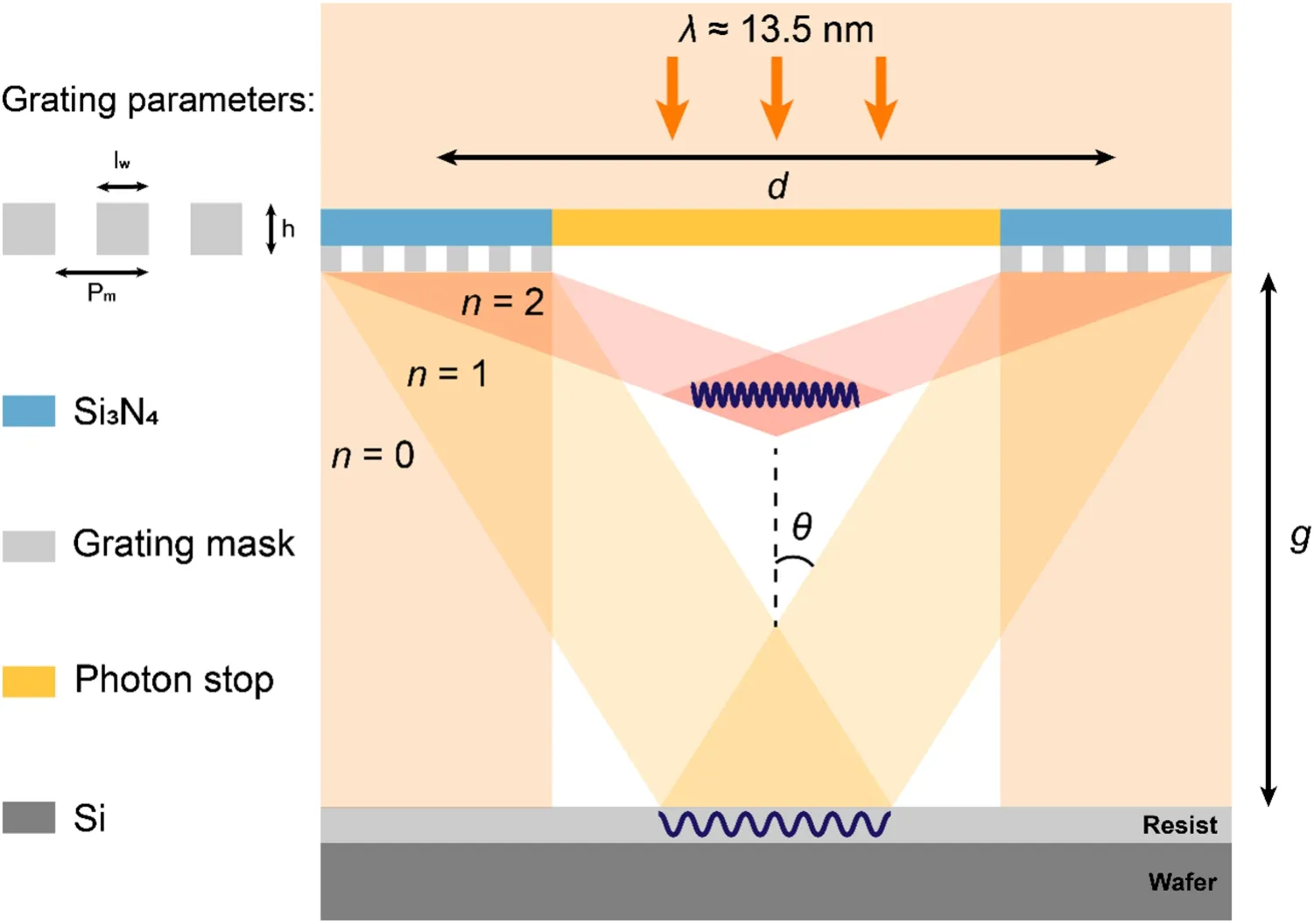
Fig.1 (Color online) EUV-IL schematic illustration.The transmission mask is vertically illuminated with EUV light and comprises gratings that diffract the coherent beam and photon stop that functions as a non-transmissive region.The two diffracted coherent beams generate interference patterns,which are recorded in the photoresist
Notably, the distance between the centers of the two diffraction gratings, denoted byd, should exceed the field area of the grating to prevent it from overlapping with the zerothorder transmitted light.The incident beam spot should fully encompass the transmission gratings to ensure the integrity of the interference.
3 Fabrication of EUV-IL grating mask
In this study, the HSQ gratings were written directly using an electron beam without pattern transfer.Gratings using highly diffraction-efficient materials can be fabricated using lift-off, etching, and electroplating processes [24].However,it is difficult to ensure a good line roughness when the period is below 60 nm.This study attempts to improve the quality of lines by reducing the number of process steps and focuses on optimizing the electron beam exposure, such as the development and exposure parameters, to fabricate HSQ gratings with periods of 60 nm and below.The repeatability of the developed process compensates for the fact that HSQ gratings are easily damaged by high-energy beam irradiation.
In conventional fabrication methods for EUV-IL grating masks, gratings are written directly onto a single silicon nitride window by electron-beam lithography, and the photon-stop layer should be precisely fabricated between two transmission and diffraction gratings, which may compromise the prepared grating structure.In this study, we propose a zoned frame with a photon-stop layer, where transmission–diffraction gratings are directly written on two separate silicon nitride windows.This effectively simplifies the mask preparation process and eliminates the influence of zeroth-order light on interference patterns.As shown in Fig.2a, 100-nm thick silicon nitride was chemically vapor-deposited on both sides of a 295-μm thick silicon at low pressure (DFS250, Calogic, Suzhou Resemi).Next, the UV photoresist (AZ 5214, AZ Electronic Materials USA Corp, Branchburg) was spin-coated at 600 rpm for 5 s and at 4000 rpm for 30 s, resulting in a UV photoresist film with a thickness of approximately 2 μm on both sides of silicon nitride.Subsequently, it was baked at 90 °C for 90 s.Two square windows with an area of 240 μm × 240 μm and a distance of 360 μm were exposed on the UV photoresist using maskless laser direct writing device (Micro Writer ML3, Durham Magneto Optics Ltd,Cambridge) at an exposure dose of 65 mJ·cm–2, followed by immersion in a developer solution (Megaposi MF-26A,Rohm and Haas Electronic Materials, Shanghai) for 45 s,rinsing in DI water for 60 s, and nitrogen blow drying.Next, a 100-nm thick silicon nitride layer was etched using an inductively coupled plasma (ICP) etch system (Plasmalab ICP 180, Oxford Instruments, Bristol).The mask frame was soaked in acetone (Sinopharm Chemical Reagent Co.Ltd..Shanghai, China) for 10 min to remove the UV photoresist, dried with nitrogen, and finally immersed in a 25% aqueous KOH solution (Sinopharm Chemical Reagent Co., Ltd..Shanghai) at 80 °C for approximately five hours.
Surface cleanliness is crucial for preparing the mask frame because it affects the uniformity of the resulting electron resist after spin coating.Therefore, prior to wet etching, the UV photoresist must be removed to prevent staining caused by its reaction with the aqueous KOH solution.Consequently, the wet-etching process removed 295-μm thick silicon, resulting in the formation of two silicon nitride windows with an area of 240 μm × 240 μm.The distance between the two windows is 360 μm,which will subsequently be utilized for the computation of the working distance g.Before spinning the electronic resist, a brief oxygen plasma treatment (Plasmalab ICP 180, Oxford Instruments, Bristol) was employed at 200 W for 10 s to cleanse the membrane surface and enhance its hydrophilicity to facilitate better adhesion of the subsequent resist application.Although the process of creating a personalized mask frame is complex, it is ideal for fabricating high-precision masks with optical requirements.
Hydrogen silsequioxane (HSQ) is widely used as a high-resolution negative resist for various applications[25].Upon exposure to high-energy electron beams,X-rays, and EUV light, it transforms into a SiO2-based structure [26].This unique property enables the direct fabrication of grating masks using EBL, and their utilization as exposed samples to evaluate the performance of EUV-IL in achieving small-scale patterns.The design of EUV-IL grating masks, written directly using an EBL with an HSQ resist, has a high degree of freedom.Various mask parameters, such as the grating heighth, line widthlw, and periodPm(Fig.1), directly impact the diffraction efficiency of the mask.Diffraction efficiency plays a crucial role in EUV-IL experiments because a lower efficiency results in extended exposure times for photoresists with equal sensitivity.This exacerbates the adverse effects of the mechanical instability on the platform and leads to blurred spatial images at the nanoscale level.The rigorous coupled-wave analysis (RCWA) method [27] is commonly employed to simulate the diffraction efficiency of such gratings, and the method has been extensively investigated.We investigated the relationship between the diffraction efficiency of nanoscale transmission gratings and material and structure using the Gsolver software based on RCWA.As shown in Fig.2b, the first-order diffraction efficiency of HSQ gratings reached its maximum when the duty cycle was approximately 0.5, which indicates that the linewidth should ideally be approximately half of the grating period.Furthermore, within a range of 100 nm,an increase in the grating height led to a corresponding increase in the first-order diffraction efficiency (Fig.2c).Notably, in terms of material selection, HSQ is the best material among the available high-resolution electronbeam resists that can be used as a mask grating directly after development.
Therefore, we established a process for creating high duty cycle, high aspect ratio HSQ gratings.Figure 3a illustrates this process.Initially, we mixed a 6% HSQ resolution concentration with H-SiOx(sourced from Applied Quantum Materials, Inc., Edmonton, Canada) and methyl isobutyl ketone (MIBK from Aladdin Biochemical Technology, Shanghai).This mixture was then spin-coated on the prepared mask frame at 4000 rpm for 45 s, achieving an approximately 90-nm thick layer.The coated frame was baked at 180 °C for 5 min.Post-baking, we observed a slight reduction in the HSQ layer's thickness due to the spin coating process.Next, we used an EBL machine(Crestec CABL-9500C, Hamamatsu City, Japan) to symmetrically write three pairs of diffraction gratings along the edge of two silicon nitride windows.The gratings had a line width of about 30 nm and a period of 60 nm, written at a beam current of 100 pA and with a dose gradient ranging from 1600 to 2000 μC?cm–2.The patterned area was then developed in a 25% tetramethylammonium hydroxide(TMAH) aqueous solution (Aladdin Biochemical Technology, Shanghai) for 45 s.Afterward, it was rinsed in deionized (DI) water for 60 s, followed by a 15-s immersion in isopropyl alcohol (also from Aladdin Biochemical Technology, Shanghai).The final step involved blow-drying with nitrogen.This process resulted in the formation of SiO2-based gratings.The final height of these gratings was slightly lower than the initial spin-coated thickness, attributable to resist shrinkage after development.
Figure 3b shows the new mask frame and overall distribution of the HSQ gratings.The photon-stop layers of silicon and silicon nitride, with a thickness of up to approximately 300 μm in the central region of the grating, provide effective shielding against prolonged exposure to high-energy beams.The area of one prepared grating was approximately 60 m × 60 m, which coincided with the size of a single EBL writing field.Furthermore, the distance between each pair of grating pairs is approximately 360 μm.Notably, the reduction in stitching errors in a 60 nm-period grating field using EBL poses a significant challenge.We observed that higher stitching errors led to spatial image distortions.To prevent distortion of the interference patterns and achieve the desired duty cycle, we utilized a single grating writing field as the EUV-IL mask and varied the dose in each writing field.As shown in Fig.4a, interior lines of gratings exhibit high contrast and low line edge roughness, and the duty cycle achieves a value close to 0.5 when a dose of 2000 μC?cm–2is administered.
The line width and period were measured using a fieldemission scanning electron microscope (FESEM, ZEISS Germany), and they corresponded to 31.63 and 61.41 nm,respectively.Additionally, identical process parameters were employed to fabricate grating masks with a period of 48 nm.A comparative analysis revealed that the inner lines of the grating exhibited increased edge roughness and reduced contrast when compared to those with a period of 60 nm,necessitating further optimization of the fabrication process(Fig.4b).Finally, to enhance the visual representation of the grating mask, we directly fabricated a 60 nm period grating with identical spin-coating parameters in the non-window region using EBL, which involved focused ion beam (FIB)slicing (Fig.4c).As shown in Fig.4d, the final grating thickness achieved a remarkable aspect ratio of approximately 3 at this structural resolution, which cannot be easily attained.Notably, the aforementioned grating characteristics not only ensure the diffraction efficiency of the grating mask but also establish favorable conditions for the transfer of other grating materials with higher diffraction efficiencies through lift-offtechnology.

Fig.3 (Color online) a First- order diffraction efficiency of different materials as a function of the period at height of 84 nm.b First-order diffraction efficiency as a function of the duty cycle at a height of 84 nm.c First-order diffraction efficiency as a function of the thickness at period of 60 nm

Fig.4 (Color online) a Interior lines of gratings with a period of 60 nm.b Interior lines of gratings with a period of 48 nm.c FIB slice of a 60-nm period grating in the non-window region.A Pt buffer layer was deposited, and the grating was sliced along line AB.(d)Cross-sectional SEM image of a 60-nm period grating.The final thickness of gratings achieved a high aspect ratio of approximately 3 with a period of 60 nm.The scale bar corresponds to 200 nm
4 EUV-IL
EUV radiation was provided by a third-generation 3.5 GeV synchrotron source (SSRF, Shanghai, China).An elliptically polarized undulator with a length of 4.2 m and period of 100 mm can provide a highly brilliant and partially coherent EUV beam with energies between 85 and 150 eV [28].A schematic of the 08U1B beamline is shown in Fig.5.A four-knife slit (Slit1) was positioned 20 m downstream from the EPU source to effectively block undesirable photons andprecisely define the acceptance angle in the horizontal and vertical directions of the beamline.The first cylindrical mirror (M1) was primarily utilized for the deflection angle adjustment, downstream thermal load reduction, and highfrequency filtration.The second cylindrical mirror (M2)reflector was placed opposite the previous mirror.Therefore,the beam had a grazing incident angle of 10o, which primarily removed high-order harmonics, adjusted the deflection,and focused on collimation.Another four-knife slit (Slit2)was positioned as a high-quality spatially coherent secondary light source for the terminal grating mask.Behind the Slit2, the mechanical shutter adjusts its opening time during exposure based on the required dose and beam flux.

Fig.5 (Color online) Schematic layout of the 08U1B beamline at Shanghai Synchrotron Radiation Facility (SSRF)
The fabricated grating mask was placed in an EUV-IL chamber located within a 100-class cleanroom (Fig.6a)and equipped with a retractable photodiode (PD) to enable precise beam flux measurements.The beam alignment and profile were finely tuned by using a charge-coupled CCD positioned at the end of the layout.The configurations of the mask and sample holder within the exposure chamber are shown in Fig.6b.Previously, we discussed the emission of gases from the EUV photoresist during the exposure process,which can cause contamination of lithography machines.The management of gas production in EUV photoresists is a critical consideration in the design and development of EUV photoresist materials, and it is an important criterion for evaluating their practicality.Additionally, at the SSRF 08U1B beam station, facilities are available for conducting outgassing detection experiments, as depicted in Fig.6e, and a mass spectrometer is used for the qualitative analysis of gas types generated during the exposure process.A highprecision ion gauge was employed to monitor the vacuum degree of the chamber in real-time, and the total amount of gas produced was quantitatively determined by calculating the changes in the air pressure before and after exposure.This method, which integrates qualitative and quantitative assessments of outgassing in diverse photoresist systems,was collaboratively developed by the Technical Institute of Physics and Chemistry (CAS) and has been successfully implemented [16].
As previously mentioned, the HSQ was used as an exposed sample to assess the efficacy of EUV-IL in realizing small-scale patterns.A 2% HSQ solution was prepared by adjusting the H-SiOx: MIBK ratio.The sample was spin-coated at 4000 rpm for 45 s to achieve a thickness of approximately 30 nm on a 400-μm thick single-side polished silicon wafer, followed by baking at 190 °C for 5 min.The low thickness of the HSQ enables optimal exposure to EUV-IL owing to its low sensitivity.The silicon wafer was positioned on the sample holder at the predetermined working distance g of 14,200 μm and irradiated at a central wavelength of 13.5 nm with a relative bandwidth of 2.38%[28].The EUV power intensity was set to 55.5 mW·cm–2with a photo flux of 1.28 × 10¹⁴photons/s and spot size of 0.15 cm2at the mask.The dose was varied from 1600 to 6700 mJ·cm–2, corresponding to exposure times between 0.5 min and 2 min.The movement of the sample holder was precisely controlled using a laser interferometer to ensure the exposure of different positions on the HSQ-covered silicon wafer to a predetermined dose gradient.After exposure,the sample was developed in a 25% TMAH solution for 45 s,followed by rinsing in DI water for 60 s, immersion in isopropyl alcohol for 15 s, and nitrogen blowing drying.

Fig.7 Scanning electron micrographs of line-space gratings with HP = 15 nm fabricated using EUV-IL on HSQ.The scale bars for different magnifications are 200 nm and 50 nm, respectively

Fig.6 (Color online) a EUVIL chamber situated within a 100-class clean room.b The configuration of the mask and sample holder within the exposure chamber.c Grating mask.d Sample holder.Observation holes are reserved.e Equipment for conducting outgassing detection experiments
The EUV exposure results are shown in Fig.7.In terms of resolution, line-space gratings with an HP of 15 nm, fabricated using an EUV-IL, were first realized at the SSRF 08U1B beam station.A periodic arrangement of interference fringes was observed in the observation area.However, it is evident that the lines are slightly blurred, indicating that the line contrast in this study has considerable potential for enhancement.These circumstances prompted the reassessment of the vibration isolation performance of an air float table carrying an EUV-IL chamber [29].After turning offpotential sources of vibration, such as molecular pumps,mechanical pumps, and air conditioners, we utilized magnetoelectric velocity probes and a data acquisition system to collect vibration data from both the ground surface and air float table surface in horizontal and vertical orientations.Their results revealed that the vibration levels on the bearing surface of the air float table exceeded those on the supporting ground.The vibration of the air float table only satisfies the VC-C standard for vibration [30], as shown in Fig.8, which significantly affects the stability of nanoscale lithography systems.The poor vibration data on the platform may be attributed to the vibrations generated by the vacuum chamber installed behind the shutter, which was used to test the beamline coherence [31, 32].Considering that we also observed the impact of mass spectrometer vibrations during exposure in previous investigations, we will proactively investigate the potential sources of vibration and uninstall idle devices that cause such disturbances.Our aim was to minimize the adverse effects of vibrations that are detrimental to high-precision exposure.Fortunately, the achievement of high-resolution patterns under such vibration conditions serves as supporting evidence for the exceptional diffraction efficiency of the grating masks.The contrast of the interference fringes can be improved by addressing these vibrational issues.
5 Conclusion
We demonstrated the capability of the SSRF 08U1B beamline to achieve fringe patterns with an HP size of 15 nm on a resist using synchrotron-based EUV-IL technology.Hence, this provided a robust assurance for the evaluation of the resolution, sensitivity, outgassing performance, and other metrics of the 5-nm node EUV photoresist.The utilization of a grating mask with high resolution and diffraction efficiency plays a crucial role in the implementation of the EUV-IL method.This prompted us to fabricate a series of high-resolution HSQ gratings with high aspect ratios using EBL on an innovative mask framework.Double-window silicon nitride substrates are suitable for achromatic Talbot imaging and multicoherent beam interference lithography because of their effective suppression of zeroth-order light.Current advancements indicate significant potential for enhancing the evaluation capability of EUV photoresists.For instance, we fabricated HSQ grating masks with a period of 48 nm on a double-window mask frame intended for use in EUV-IL experiments to achieve high-resolution fringe patterns.Further optimization is necessary to improve the line contrast of the 48-nm periodic grating mask.Additionally, the practicality of the grating masks can be enhanced by improving the larger-field writing capability of highresolution structures using EBL, which expands the surface area covered by a single grating.Spatial image distortion resulting from stitching in the writing field can be effectively mitigated in this manner, thereby enhancing the coverage of the interference zone patterns.This enables greater flexibility in adjusting the working distance g and facilitates easier observation of the interference fringe patterns.Furthermore,to address vibration issues, we strictly monitored known sources of vibrations, such as molecular pumps, mechanical pumps, nearby air conditioners, and fans, during each exposure experiment.Moreover, we will conduct comprehensive vibration detection of the surrounding environment of the interference lithography experimental chamber.In the future, we plan to use an improved active antivibration exposure chamber platform to minimize the adverse effects of vibrations on high-precision exposure.
Acknowledgements The authors are grateful to the staffof the BL08U beamline at SSRF.
Author contributions All authors contributed to the study conception and design.Material preparation, data collection and analysis were performed by Zhen-Jiang Li, Cheng-Hang Qi, Bei-Ning Li, Shu-Min Yang, Jun Zhao, Zhi-Di Lei, Shi-Jie Zhu, Hao Shi, Lu Wang,Yan-Qing Wu and Ren-Zhong Tai.The first draft of the manuscript was written by Zhen-Jiang Li and all authors commented on previous versions of the manuscript.All authors read and approved the final manuscript.
Data Availability The data that support the findings of this study are openly available in Science Data Bank at https:// doi.org/ 10.57760/ scien cedb.j00186.00344 and https:// cstr.cn/ 31253.11.scien cedb.j00186.00344.
Declarations
Conflict of interest Ren-Zhong Tai is an editorial board member and was not involved in the editorial review, or the decision to publish this article.All authors declare that there are no competing interests.
 Nuclear Science and Techniques2023年12期
- Nuclear Science and Techniques的其它文章
- A machine learning approach to TCAD model calibration for MOSFET
- BL02U1: the relocated macromolecular crystallography beamline at the Shanghai Synchrotron Radiation Facility
- Coin-structured tunable beam shaping assembly design for accelerator-based boron neutron capture therapy for tumors at different depths and sizes
- Simulation study of BESIII with stitched CMOS pixel detector using ACTS
- Advances in nuclear detection and readout techniques
- Enhancing betavoltaic nuclear battery performance with 3D P+PNN+multi-groove structure via carrier evolution