
Macro Meso Response and Stress Wave Propagation Characteristics of MCT High-Voltage Switch Under Shock load
2024-03-20 06:43YuyangGuoChuangChenRuizhiWangEnlingTang
Defence Technology 2024年2期
Yuyang Guo, Chuang Chen, Ruizhi Wang, Enling Tang
Key Laboratory of Transient Physical Mechanics and Energy Conversion Materials of Liaoning Province, Shenyang Ligong University, Shenyang,110159,Liaoning, China
Keywords:MCT Impact load Failure analysis Stress wave Numerical simulation
ABSTRACT In order to study the dynamic and electrical coupling response characteristics of Metal Oxide Semiconductor Controlled Thyristor (MCT) high-voltage switch under the synergic action of mechanical load and high voltage, the separated Hopkinson pressure bar (SHPB) test system was used to simulate different impact load environments, and combined with the multi-layer high-voltage ceramic capacitor charging and discharging system, the instantaneous electrical signals of MCT high-voltage switch were collected.Combined with numerical simulation and theoretical analysis, the failure mode and stress wave propagation characteristics of MCT high voltage switch were determined.The mechanical and electrical coupling response characteristics and failure mechanism of MCT high voltage switch under dynamic load were revealed from macroscopic and microscopic levels.The results show that the damage modes of MCT high-voltage switches can be divided into non-functional damage,recoverable functional damage,non-recoverable damage and structural damage.Due to the gap between the metal gate and the oxide layer, the insulating oxide layer was charged.After placing for a period of time, the elastic deformation of the metal gate partially recovered and the accumulated charge disappeared, which induced the recoverable functional damage failure of the device.In addition,obvious cracks appeared on both sides of the monocrystalline silicon inside the MCT high-voltage switch, leading to unrecoverable damage of the device.
1.Introduction
With the rapid development of microelectronic technology,the intelligence and multifunction of missile-borne weapon systems has become an obvious development trend.The initiation control system is an important part of the internal fuze of the projectile.Identifying and processing the penetration information is its main function, which determines the optimal initiation position and complete the initiation task of the warhead.The key components in the projectile body often experience multiple impact loads before the initiation task has been performed.After the fuze is released into the standby state,ignition energy is stored by the high-voltage capacitor, and the high-voltage switch controls the energy release channel.Due to the high voltage of thousands of volts on the nanometer scale, the electrical field strength reaches the order of magnitude of 108V/m.These key components will show different physical characteristics from the conventional low-voltage devices.In terms of mechanical characteristics,when the fuze is excited by a strong mechanical load, the internal structure of the MCT with brittle semiconductor material as the core will deform and vibrate at a high frequency.In terms of electrical characteristics, there are transient fluctuations of voltage and current;Meanwhile,under the combined interaction of high voltage and dynamic load, complex electromechanical coupling response and failure will occur.Since the missile-borne devices have high requirements for safety and reliability, the synergistic effect of high-voltage and severe high overload environment will seriously affect the working efficiency of the fuze system, and even lead to safety and reliability problems such as an early explosion or dumb bomb.How to effectively detect the stability of the function of key electronic components in the system under extremely complex environment, and the study of multi-scale mechanical induced damage determination in complex structures is rarely reported.
MCT high-voltage switch plays a key role in the initiation controller.The advantage of the MCT high voltage switch lies in that the conventional MOS gate control signal can be used to control the switch,and the pulse peak current can reach thousands of amperes in a hundred nanosecond, and the voltage withstanding can be blocked forward for thousands of volts, which can be used for nondestructive testing.Therefore, MCT is suitable for ignition and initiation systems.In recent years, there are many reports on the application of MCT in capacitor discharge units and in-line electronic security systems in foreign countries.In 2002,Hanks R L[1]used MCT to control high-voltage capacitor discharge.In 2008,Kluge Design Inc (KDI) [2] announced the Multiple Launch Rocket System(MLRS)using the linear electronic security system and lowenergy explosive foil initiator.In 2010, Barham O [3] published an all-electronic device for an electronic security system developed by the United States Army,which used MCT as its high voltage switch.In 2016, Max P [4] pointed out in the research progress of lowenergy explosive foil that semiconductor switches, such as MCT,will gradually replace spark gap switches in the future.In 2017,Michael D [5] proposed a small electronic security system, which realized the planarization of an electronic security system (about 10 cm2)by using commercial MCT and promoted the development of a low-energy explosive foil initiation system.In 2017, He S M et al.[6]studied the discharge characteristic curve of the capacitor discharge unit (CDU) short circuit and access to the explosion foil.The successful initiation of the two-way impactor detonator was realized, and the synchronous dispersion was less than 100 ns.At present, MCT high-voltage switch has an important application value in the ammunition system.However, with the gradual deepening of engineering applications, it is necessary to further study the electro-mechanical response of MCT high-voltage switching under the synergistic effect of high voltage and dynamic load.In particular, the electro-mechanical response of MCT high voltage switch under different impact loads is studied to reveal the physical mechanism of functional damage in extreme environments.
MCT high-voltage switch is composed of multi-layer media.This structural feature will lead to extremely complex stress wave propagation.Profoundly revealing the propagation characteristics of stress waves in MCT high-voltage switch under high overload will clarify the physical mechanism of device damage.Many scholars have performed a series of related researches on the dynamic response and failure of electronic packaging devices or multilayer structures under strong impact loads.Li L et al.[7]conducted a high g value experiment on the crystal oscillator chip by using the Hopkinson pressure bar and estimated the overload acceleration of the chip by using the one-dimensional stress wave theory.The experimental results show that the impact resistance of the chip placed parallel to the stress wave propagation direction is higher than that of the chip placed perpendicular to the stress wave propagation direction.Xu P[8] studied the impact performance of two kinds of crystal vibrations commonly used in missile-borne storage test circuit modules under the condition of encapsulation and without the use of epoxy resin glue.The experimental results show that the impact resistance of epoxy resin-filled crystal vibration is not significantly higher than that of unfilled crystal vibration; Dong Y X et al.[9] carried out a low-velocity impact test and corresponding numerical calculation.The influence of a multilayer medium with different structures on the propagation of stress waves was analyzed.The experimental results show that the action time of stress wave is not only related to the medium composed of a multilayer medium but also the thickness of the medium, the impedance matching of the composite medium, and the wavelength of the incident wave.Huang W et al.[10] studied the deformation and failure of a single component by threedimensional digital imaging technology, focusing on the influence of load strength,structural performance and load conditions.It was found that the main failure mode changed from core fracture and inelastic deformation to crack and fracture with the increase of external pulse and internal density of interlayer.Robbins J R et al.[11] used numerical simulation to study the influence of layer damage and the defect interface of load diffusion.The results show that the medium with different impedance enhances the penetration resistance of the target through the combination of various mechanisms.Hassani S et al.[12]used the finite element model to study the stress distribution in the multilayer coating.The simulation results show that Young’s modulus of the top layer of the multilayer medium plays an important role in the stress distribution.When the top layer of the multilayer medium has a relatively low Young’s modulus,compressive stress occurs in the coating,and when the top layer has a high Young’s modulus, tensile stress occurs in the coating.Meo M et al.[13]simulated the generation and expansion of engine fan casing damage by using kinetic energy projectile impacting on sandwich structure at low speed and analyzed the energy absorption characteristics of the structure.Li J et al.[14] studied the reliability of Micro-Electro-Mechanical System (MEMS) by combining a pneumatic impact tester and finite element simulation.The damage location observed by the simulation results effectively verified the failure mode of MEMS in experiment and effectively predicted the potential damage at the interface.Zhang H et al.[15]used the stress wave theory to analyze the dynamic behavior of lithium-ion batteries and simulated the crushing behavior at 45 m/s impact velocity.Li S [16,17] analyzed the mechanical behavior of specimens under different loads by combining theoretical derivation, experimental measurement and numerical simulation, and verified the feasibility of such research methods.Chen Y et al.[18] collected the change process of temperature and voltage during the impact process of lithium batteries through experiments.The influence of contact between different layers of electrodes and separators was simulated.Li L et al.[19]proposed the mechanism behind the characteristic degradation from the total ionization dose damage in the anode-short MCT from a device physics perspective.Xi S J et al.[20] established a battery computational model for analyzing the mechanical response of the battery based on the experiment.The related results could provide a reference for the safety design of the battery under the mechanical integrity framework.Li L et al.[21] proposed the mechanism behind the characteristics degradation from displacement damage in trench field-stop reverse-conducting IGBT from a device physics perspective.The dependencies of the key parameters on neutron fluence were analytically modeled.In summary,there is no relevant report on the electro-mechanical response of MCT highvoltage switch subjected to strong impact load in the working process.It is necessary to conduct the study on the electromechanical response law of MCT high-voltage switch under the synergistic effect of different stress pulse amplitudes and determine the failure mode.Moreover, the physical mechanism of MCT high voltage switch failure under electro-mechanical synergistic action remains to be revealed.
In this paper,experiments,numerical simulation and theoretical derivation are combined to study the reliability of MCT highvoltage switch under the synergistic action of impact load and high-voltage charging.Based on the constructed SHPB experimental system,the dynamic stress-strain relationship of MCT highvoltage switch under impact load is tested,and the output electrical signals before, during and after impact are collected.By using Abaqus software, finite element simulation of MCT high-voltage switch in the process of impact loading is carried out to analyze the stress distribution and failure mechanism inside the device in the process of impact loading.Combined with one-dimensional stress wave propagation theory, stress wave propagation in variable section is deduced.The mechanical and electrical coupling response characteristics and failure mechanism of MCT high voltage switch under dynamic load are revealed from macroscopic and microscopic levels.
2.Experiments
2.1.Cellular structure and electromechanical parameters of MTC high voltage switch
The main body of the MCT high-voltage switch is the thyristor,and its top control part includes two Metal-Oxide-Semiconductor Field-Effect Transistors (MOSFETs), which belong to bipolar devices.The MCT high-voltage switch model selected in this paper is MCT14BZDHCL026,and the physical diagram is shown in Fig.1(a).The withstanding voltage value of the device is 1400 V, and the repetitive pulse current is 3500 A,which has the characteristics of a constant switching function.The opening mechanism of MCT is similar to that of Insulated Gate Bipolar Transistor (IGBT).By applying a positive gate voltage, N-Metal-Oxide-Semiconductor(NMOS) is turned on.The electronic current of NMOS flows to the base area of the PNP transistor, which is used as the base driving current to turn on the PNP transistor.The collector current of the PNP transistor is used as the base driving current of the NPN transistor to turn on the NPN transistor.The regeneration mechanism of positive feedback is formed between the two coupled transistors,and the MCT thyristor maintains the conduction mode.To turn off the MCT in the on-state,negative bias voltage should be added to the gate.At this time, p-channel MOS will be formed on the surface of the n-emitting region.The holes in the p-base region flow to the cathode through the p-channel MOS,which reduces the excess holes in the p-base region and causes the positive bias of the emitter to decrease until the injection efficiency of the emitter is zero, and the device stops the positive feedback.Since then, the device can be equivalent to an open-circuit PNP transistor,and the excess carriers in the n-base region disappear gradually through recombination until the device is turned off.The cell structure diagram of MCT is shown in Fig.1(b).The structure diagram of MCT is shown in Fig.1(c).
The MCT is composed of five layers, namely Epoxy resin,Aluminum 1015, SiO2, Si and Cupronickel.During the experiment,the MCT is fixed on the Printed circuit boards(PCB).To improve the smoothness of the device surface, the beam pressure of the solder joint is reduced to the PCB surface, and the uneven stress distribution is reduced.During the impact process, the bias voltage of MCT is 10 V,leakage and source short circuit grounding.Table 1 is the material parameters of MCT and PCB.Table 2 is the electrical parameters of MCT.
2.2.Experimental installation
2.2.1.Charging and discharge control circuit

Fig.1.MCT and cell structural diagram: (a) MCT Welded on PCB; (b) MCT cell structural diagram; (c) Structure diagram of MCT.

Table 1 MCT and PCB material parameters [22-28].
Based on FPGA(Field Programmable Gate Array)technology,the Capacitor Discharge Unit (CDU) (Fig.2(a)) is developed.VHDL programming language is used to control the circuit board port to realize the charging and discharging process of a high voltage circuit.The low-power direct current power supply is used to supply power to the FPGA microcontroller chip,and the FPGA receives and judges the command signal of the host computer.After meeting the requirements, the dynamic switch is opened, the MOSFET conduction charging circuit is started, and the high voltage power supply is charged to the multi-layer ceramic capacitor.Meanwhile,the charging feedback signal is provided to the FPGA chip.After charging, the MCT conduction is controlled.At this time, MCT,multi-layer ceramic capacitor and discharge circuit resistance are composed of a series discharge circuit.The capacitance value of many ceramic capacitors is 1 μF and the voltage value is 1400 V.Fig.2(b)is the circuit of the dynamic monitoring system,Fig.2(c)is the schematic diagram of the charging and discharge circuit and the electrical signal acquisition system,where u1and u2are drivers and Fig.2(d) is the equivalent circuit diagram of discharge circuit.
Considering the dramatic change of the circuit current in the discharge process will induce a high current change rate di/dt,the parasitic inductance and parasitic capacitance inside and outside the gate will induce jitter voltage at high di/dt,and the jitter voltage is likely to exceed the gate withstand voltage value, resulting in MCT damage, hence the Transient Voltage Suppressor (TVS) isparalleled at both ends of the gate and the gate return pole of MCT to prevent the impact of gate voltage jitter on MCT.The fast recovery diode (FRD) is inversely paralleled at both ends of the ceramic capacitor, and the reverse current generated in the discharge stage of the capacitor can be continued through the FRD,rather than through the MCT cathode and anode, thus protecting from the MCT.Therefore, FRD maintains the unidirectional conduction characteristics of MCT during the whole circuit discharge[29],which is shown in Fig.2(d).According to Kirchhoff voltage law,when the capacitor voltage u(t) is positive, the discharge process can be described by zero input response Eqs.(1)and(2)of the R-L-C series circuit.

Table 2 Electrical characteristics of MCT.

Fig.2.Charging and discharge control circuit:(a)Capacitance charging and discharge unit;(b)Dynamic monitoring system;(c)Chart of charging and discharge circuit and electrical signal acquisition system; (d) Equivalent circuit diagram of the discharge circuit.

In Eq.(6),u(0)is the initial discharge voltage of the capacitor,u(t)is the capacitance voltage,the initial discharge current of the circuit is zero,i(t)is the discharge current,R is the circuit resistance,L is the inductance and C is the capacitance.
The output voltage ranges from 1270 to 1300 V in the experiment.The charging time of a multi-layer ceramic capacitor can be expressed as
In Eq.(7),u(a)is the voltage value of the capacitor charging,t is the charging time, R1is the charging circuit resistance, and the resistance value is 250 Ω.The initial voltage of the capacitor is zero,and the voltage is 1270 V after charging.The charging time can be completed when the charging time exceeds 3-5 RCs, and the charging time of each experiment exceeds 5 RCs.
The voltage value and discharge duration during capacitor discharge can be calculated by Eqs.(8) and (9), and the longest discharge duration is about 0.06 ms.
In Eqs.(8)and(9),R2is the discharge circuit resistance and the resistance value is 30 kΩ.
2.2.2.SHPB experimental system
The dynamic stress-strain relationship and electrical output characteristics of the MCT high-voltage switch under impact load are tested by SHPB experimental system.The experimental device is shown in Fig.3.The experimental device is composed of a bullet,incident bar and transmitted bar, and the diameters are 16 mm.Since the specimen may be short-circuit under a strong dynamic load,the specimen is placed in the test box.The holes on both sides of the test box ensure that the bar passes through without friction,and several layers of kraft paper are placed at the bottom of the box and being used as insulation.The dynamic strain gauge was used to record the strains of MCT during the experiment.The dynamic response image of the MCT high-voltage switch under dynamic load was collected by PCO.dimaxHS4 high-speed camera and the frame rate was set as 46,746 fps.In the experiment, the control circuit board and the oscilloscope were triggered in a synchronous mode.The trigger signal is used as the synchronous trigger source to coordinately control the synchronous operation of the circuit board and the oscilloscope (voltage probe and current probe).
2.2.3.Basic experimental parameters
Six experiments were carried out to collect the output electrical signals(current and voltage in the discharge circuit)before,during and after the impact.Meanwhile, the time history curves of stress and strain of the specimen during the impact process are obtained by a dynamic strain gauge.On the premise of ensuring the safety of the experimental process, PMMA and Dilecto were selected as bar materials, respectively.The material parameters of the bars are shown in Table 3.
In Eq.(10), L is the bullet length and C1is the elastic wave velocity of the bullet material.According to Eq.(10), the duration of the loading pulse is 0.15 ms.The loading pulse time is longer than the capacitor discharge time, which can ensure that the whole discharge process is within the pulse duration of the stress wave.The propagating time of the stress wave from the contact interface between the incident bar and the specimen is 0.37 ms.The dynamic strain gauge starts to work when the head wave is received by the strain gauge, and the strain gauge is in the middle of the incident bar.To achieve the discharge of the control circuit in the process of stress pulse interaction,the conduction time is delayed by 0.42 ms when the synchronous trigger is made, that is, the circuit is switched on and discharged after 0.05 ms of the stress interaction specimen.After many tests,it is determined that the discharge time can be realized within the duration of the head wave pulse under this delay time.
When the bar material is Dilecto, the bullet length is 200 mm,and the lengths of the incident and the transmitted bar are 1200 mm.The pulse duration can be calculated by Eq.(10) to be about 0.30 ms.When the stress wave propagates from the contact interface between the bullet and the incident bar to the interface between the incident bar and the specimen, the time required is 0.91 ms,hence the circuit conduction time is delayed about 1.0 ms when the synchronous trigger is made,that is,after the stress pulse acting on the specimen 0.09 ms,the circuit discharges.After several tests, it is determined that the discharge time can be achieved within the duration of the first stress wave pulse under this delay time.

Fig.3.Schematic diagram of SHPB experimental device.

Table 3 Material parameters.
The electromechanical response characteristics of MCT under different stress pulses are determined by changing the velocity of the bullet.Table 4 is basic parameters in experimental Nos.1-6.The mechanical response parameters (stress peak, strain peak,strain rate), electrical output characteristics (peak current), and device function test results of the specimen are shown in the table.(Because the overall structure of MCT was seriously damaged during the experimental No.6, the super dynamic strain gauge failed to record the complete data)
3.Result and discussion
3.1.Electromechanical response characteristics of MCT high-voltage switch under impact load
Based on the test results of device function after experiment,the damage modes of MCT high-voltage switch under impact load are divided into non-functional damage (Experimental No.1), recoverable functional damage (Experimental No.2, No.3), unrecoverable functional damage(Experimental No.4,No.5),and structural damage (Experimental No.6).The electromechanical response characteristics of specimens under four damage modes were analyzed.
3.1.1.Non-functional damage
By comparing the electrical output signals before, during and after the impact in experimental No.1, it is found that there is no obvious fluctuation in the electrical output signal, indicating that the specimen has no functional damage under this overload and can work normally.Fig.4 is the discharge signal and time-history curve of stress-strain in experimental No.1.
During the action of head wave stress pulse, MCT and PCB are deformed as a whole,and the maximum axial deformation is about 0.16 mm.In the first 0.06 ms when the stress pulse starts to act on the device,the current and voltage changes in the circuit have good synchronization,and the impedance stability in the circuit is about 30.36 kΩ;In the process of 0.06-0.105 ms,with the increase of the stress acting on the device,the device strain increases from 0.0195 to 0.0249,and the deformation is about 0.14 mm.The impedance in the circuit begins to decrease gradually with the increase of the device strain, and the impedance in the circuit is 27.93 kΩ at the moment of 0.0885 ms.This physical mechanism can be explained that the strain generated by the device will induce the change of the carrier concentration in the internal semiconductor.After 0.105 ms,the strain of the device increases from 0.0249 to 0.0266, and the overall deformation of the device is 0.16 mm, however the impedance in the circuit remains stable.
3.1.2.Recoverable functional damage
It is found that when the peak stress reached 41.70-46.70 MPa,the electrical output signal of the MCT high-voltage switch wasabnormal during the process of impact.The device after impact was immediately tested, and the electrical output signal of the device was still abnormal,but the device was not significantly damaged.In addition, the MCT high-voltage switch was tested after remaining 5min, and the function of switch returned to normal.The above phenomena occurred in the repetitive experimental Nos.2 and 3,and the damage model of the specimen under this overload was determined to be the recovery after a transient fault.Taking the experimental No.2 as an example, the time history curves of discharge signal, stress and strain after impact neutralization are shown in Fig.5.
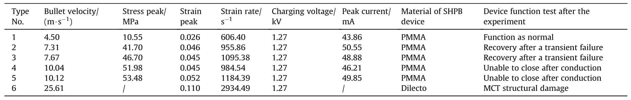
Table 4 Experimental basic parameters.

Fig.4.Time history curves of discharge signals, stress, and strain during impact in experimental No.1.
Before impact, the discharge process of MCT was tested.The voltage in the circuit was 1.27 kV, and the discharge current reached the peak value at the moment of 0.002 ms after conduction, the peak current and discharge duration were 44.52 mA and 0.06 ms,respectively.As shown in Fig.5(a),the stress and strain of MCT during conduction were 28.92 MPa and 0.031, respectively.After conduction, the current reached the peak value at the moment of 0.002 ms and then decreased gradually.The peak current was 50.55 mA, and the stress and strain were 29.58 MPa and 0.0318, respectively.Within 0.05 ms after conduction, the current and voltage in the discharge circuit did not decrease to 0 in time,but there was still a downward trend.When the stress load of MCT is 37.79 MPa and the strain is 0.035,the current and voltage in the discharge circuit stop decreasing and show an upward trend,which proves that the MCT has functional failure under this load, and cannot hold the voltage at both ends normally,and the failure does not disappear immediately after the load is unloaded.
During impact, the stress of the specimen reached the peak at the moment of 0.08 ms after conduction,and the stress and strain were 41.70 MPa and 0.0374, and the current and voltage in the discharge circuit were 38.65 mA and1.08 kV, respectively; the specimen produced the maximum strain at the moment of 0.15 ms after conduction, and the strain and stress were 0.046 and 21.77 MPa, the current and voltage in the discharge circuit were 44.62 mA and 1.28 kV, respectively.The internal carrier concentration changed and then the circuit impedance changed due to the deformation of the MCT high-voltage switch during the interaction of stress pulse.At the moment of 0.094 ms before the stress pulse interaction, the strain of the device increased sharply from zero to 0.034, but the internal resistance of the device did not change significantly.When the overall strain and deformation of the device is 0.034 and about 0.21 mm, respectively.With the change of the strain of the circuit impedance decreases by 2.03 kΩ.When the strain of device was stable at 0.046 and the deformation was 0.28 mm,the circuit impedance also stopped changing,meanwhile it was 2.04 kΩ, which was less than the initial circuit impedance.
The electrical output signals of the MCT high-voltage switch tested immediately after shock and after remaining 5 min were shown in Fig.5(b) and 5(c), respectively.From the results of mechanical and electrical response, it could be seen that the multilayer structure of MCT produces elastic deformation under impact load.When the strain was 0.0358, the MCT produced functional damage.After unloading, the elastic deformation of the device could not be restored immediately, and the discharge signal was abnormal.After remaining 5 min, the elastic deformation of MCT was restored.The electrical parameters after conduction were consistent with those before impact, and it was judged that the device had returned to a normal working state.
The internal defects of the MCT high-voltage switch after impact were detected by SAM, and the internal structural changes of the specimen were analyzed by C phase diagram and T-scan image,so as to clarify the damage mechanism of the specimen.The scanning sampling frequency of the microscope is 15 MHz, and scanning speed of X and Y are 200 mm/s, respectively.Fig.6 shows the acoustic image and scanning waveform in experimental No.2 specimen.

Fig.5.Discharge signals after impact neutralization and time history curves of stress-strain:(a)Time history curve of discharge signal and stress-strain during impact;(b)Discharge signals Collected before impact; (c) Discharge signals of acquired after shock; (d) Discharge signals collected aftershock 5 min.
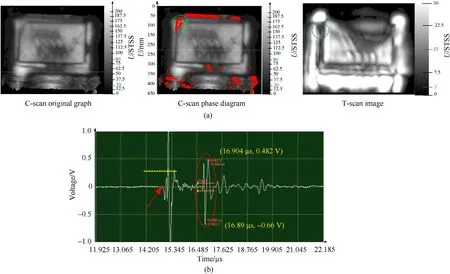
Fig.6.Acoustic image and scanning waveform in experimental No.2 specimen: (a) SAM acoustic image; (b) SAM scan waveform.
In Fig.6(a),the entire red coloring region of the C phase diagram was a layered region,and the green ring in the C phase diagram and the T-scan image was a layered region of the internal structure of the device.The scanning waveform of the MCT inner delamination area (green circle area + A _ 3) was shown in Fig.6(b).The red arrow in the scanning waveform was the starting point.The waveform was the surface wave from the coupling agent to the epoxy resin interface, which was from low impedance to high impedance.The waveform at the moment of 16.73 μs was the waveform from the epoxy resin to the MCT inner chip interface,which was still from low impedance to high impedance.In the detection area, the waveform presented a sine wave state of two cycles, which proved that the MCT inner chip appeared delamination at this point and the overall waveform was complex.Combining the acoustic scanning image and scanning waveform,it could be determined that there was structural stratification within the device;In addition,there was no bubble zone during the whole scanning process, which proved that the overall material of the device did not appear damage and the package was complete.The transient fault recovery mechanism of the device could be explained as the damage caused by the internal structure stratification of the device.
3.1.3.Unrecoverable functional damage
With the increase of the bullet speed, when the peak stress reached 51.98-53.48 MPa, the data collected by the dynamic monitoring system showed that the MCT high-voltage switch produced irreversible damage during impact.After unloading, the electrical output signal was still functional damage of the display device after remaining 5 min, and there was still no structural damage on the surface of the device.This phenomenon was found in repeated experiments of No.4 and No.5,and it was determined that the damage mode of the specimen under this overload was unrecoverable functional damage.Taking the experimental No.5 as an example,the time history curves of discharge signal,stress and strain during impact are shown in Fig.7.
During the process of impact, the stress and strain of MCT conduction were 36.15 MPa and 0.0347, respectively.After conduction,the peak current was 49.85 mA at the corresponding to the moment of 0.002 ms,and the stress and strain were 37.59 MPa and 0.0375;at the moment of 0.05 ms after conduction,the current and voltage in the discharge circuit increased twice,and the current and voltage were 36.15 mA and 1.02 kV, the stress and strain of the specimen were 48.47 MPa and 0.0374,respectively;at the moment of 0.13 ms after conduction,the current and voltage in the discharge circuit were stable.At this time, the current and voltage were 44.76 mA and 1.27 kV, the stress and strain of the specimen were 48.41 MPa and 0.049, respectively.
During the process of impact,the stress of the specimen reached the peak at the moment of 0.07 ms after conduction,and the stress and strain were 53.48 MPa and 0.0374, the current and voltage in the discharge circuit were 37.71 mA and 1.06 kV, respectively; the specimen produced the maximum strain at the moment of 0.14 ms after conduction, and the strain and stress were 0.052 and 32.99 MPa, the current and voltage in the discharge circuit were 44.80 mA and 1.27 kV,respectively.When the impact velocity was large, the stress wave acted on MCT, and the strain of the device increased from zero to 0.0372 within 0.05 ms.When the circuit started to turn on,the deformation of the device was 0.23 mm,and the impedance in the circuit decreased by 2.04 kΩ;The maximum deformation of the device during the whole loading process was 0.33 mm,and the impedance in the circuit decreased by 2.52 kΩ.It could be clearly seen from the time history curve of strain in the range of 0.06-0.12 ms, the overall strain of the device decreased slightly with the increase of stress,which may be the fully failure of the device due to a certain gap in the packaging process.The yield stage occurred between 0.10 ms and 0.14 ms.Fig.8 was the local magnification of the MCT high-voltage switch after impact,and the red arrow direction was the impact loading direction.It could be observed that the Epoxy resin package and Cupronickel were intact after impact.
Fig.9 showed the acoustic image and scanning waveform in experimental No.5.According to the acoustic scanning photos, as shown in Fig.9(a), the whole red coloring area in the C phase diagram was the damaged area, and the green ring was the internal damage area of the device.The scanning waveform of the MCT internal damage zone (green circle area + A _ 1) was shown in Fig.9(b).The red arrow in the scanning waveform was the starting point.This waveform was still the surface wave from the coupler to the epoxy resin interface, which was from low impedance to high impedance.The waveform at the moment of 16.96 μs was the waveform from the epoxy resin to the MCT internal chip interface,which was still from low impedance to high impedance.However,the waveform at this point was negative, which proved that the crack damage occurred in the MCT internal chip.It was determined that the unrecoverable functional damage of the device was caused by the crack of the internal chip under impact.

Fig.7.Time history curve of discharge signal, stress and strain during impact in experimental No.5.
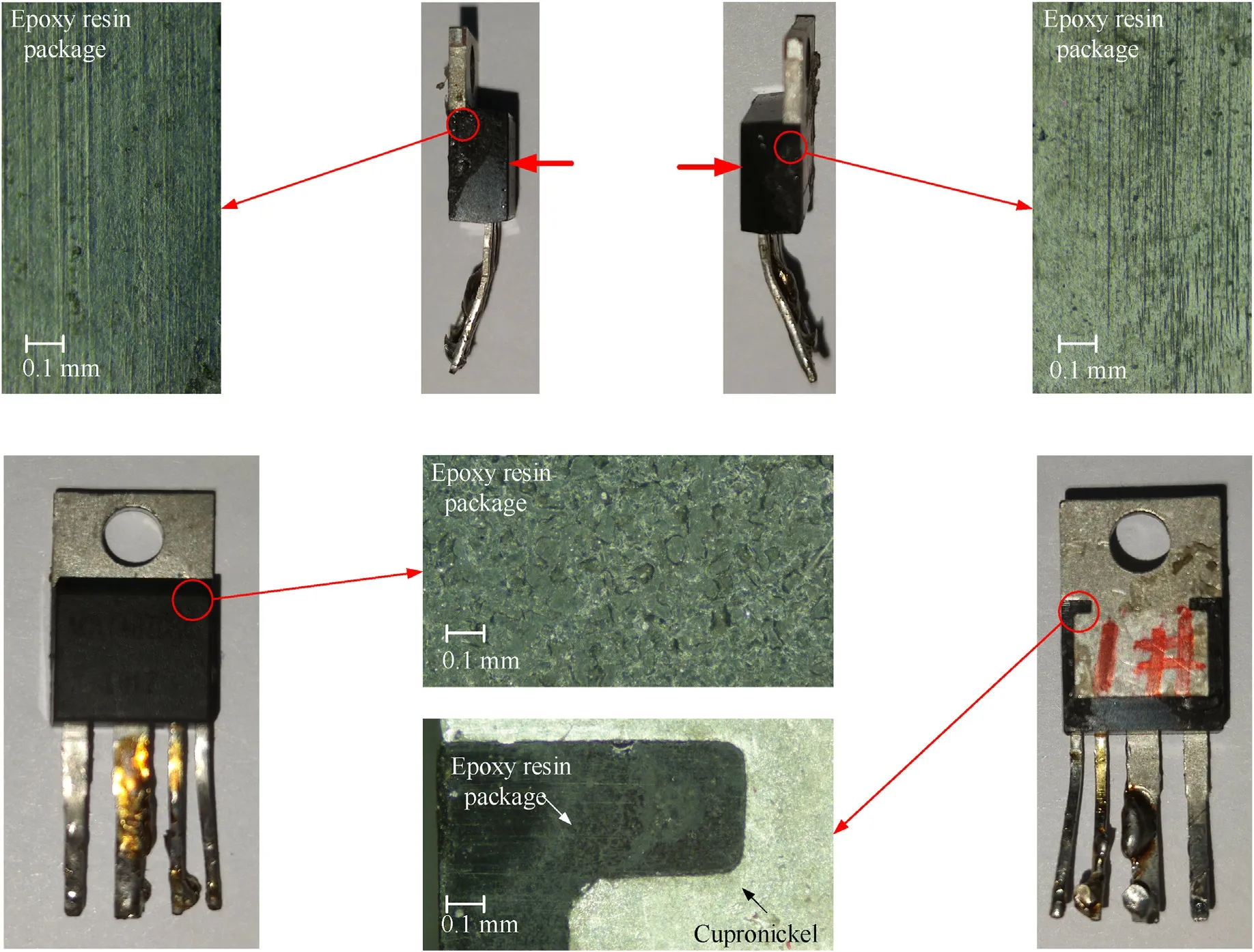
Fig.8.Local amplification diagram of MCT high-voltage switch after impact.
Fig.9.Acoustic image and scanning waveform in experimental No.5: (a) SAM acoustic image; (b) SAM scan waveform.
3.1.4.MCT structural damage
In experimental No.6, the overall structure of the MCT highvoltage switch was damaged when the bullet velocity was 25.61 m/s,as shown in Fig.10.It could be seen from the figure that the external epoxy resin layer had a serious crack phenomenon,which was caused by the interaction between the incident loading stress pulse head and the unloading wave at the tail of the incident loading stress pulse after the reflection of the incident loading stress pulse head on the free surface as the unloading carrier.The stress pulse was reflected many times on the free surface to form a tensile wave,and the tensile stress generated was greater than the tensile strength of epoxy resin to induce delamination.
The breaking process of the MCT high-voltage switch recorded by a high-speed camera was shown in Fig.11.

Fig.10.MCT structural damage.
By comparing the results in experimental Nos.1-6, when the overall strain of the MCT high-voltage switch was less than or equal to 0.026, the peak stress was less than or equal to 10.55 MPa, it would not have any effect on the function of the device.When the overall strain of the MCT high-voltage switch was in the range of 0.045-0.046, and the peak stress was in the range of 41.70-46.70 MPa,the transient fault recovery would occur,and the function of the device would return to normal after 5 min.According to the scanning results of ultrasonic microscopic scanning technology, it was judged that the transient fault recovery of the device was caused by the elastic deformation generated during impact, and the internal delamination occurred.When the elastic deformation of the device was restored,the electrical output signal was normal; When the overall strain of the MCT high-voltage switch was in the range of 0.046-0.052, the peak stress was in the range of 51.98-53.48 MPa, the unrecoverable functional damage would occur, and there was no damage outside the device.According to the acoustic microscope scanning results, it was judged that the unrecoverable functional damage was caused by the chip damage inside the device.When the bullet velocity was greater than 25.61 m/s, the structure damage would occur.
3.2.Numerical simulation of mechanical response of MCT highvoltage switch under impact load
According to the electrical signals collected in experiments, it could be seen that different damage modes of MCT high-voltage switch showed different turn-off abilities.However, the experiment could only observe the occurrence of damage from a macro point of view, and can not profoundly reveal the internal physical mechanism.Therefore, Abaqus software was used to explore the physical essence of functional damage caused by the MCT highvoltage switch during impact load.
3.2.1.Establishment of finite element model
Since the MCT high-voltage switch belonged to a multi-layer structure, the propagation of the stress wave inside device involved in the reflection and transmitted wave at the interface.The experiment could only obtain the overall stress and strain of the packaging device.Combining with the numerical simulation of MCT high-voltage switch under strong dynamic load,the stress and strain changes of each layer medium were analyzed,and the reason for the functional damage was further deduced.To be consistent with the experimental conditions,PCB was added to the simulation,and the simulation model was shown in Fig.12 [31-33].

Fig.11.Crushing process of MCT high-voltage switch under impact load: (a) t = 0 ms; (b) t = 0.10 ms; (c) t = 0.20 ms; (d) t = 0.30 ms.
The geometric model of each part of MCT was performed by Abaqus internal component module.The thickness of the SiO2layer was 40 nm, and the geometric size difference of other parts was large.Therefore,the three-dimensional shell was used to model it.The thickness of the shell unit was set to 40 nm, and the threedimensional variable row body is used to model the material.The approximate global mesh sizes of Epoxy resin, Aluminum,SiO2, Si,Cupronickel,PCB and bar were 0.51 mm,0.1 mm,0.1 mm,0.08 mm,0.5 mm, 1 mm and 2.3 mm, respectively.The wave impedance relationship of MCT components was:Cupronickel> Si > Aluminum 1015 > SiO2>Epoxy Resin.
3.2.2.Accuracy verification of numerical simulation
To verify the accuracy of numerical simulation results,the stress nephogram of the MCT high -voltage switch was collected by DIC technology in experimental No.5.Figs.13 and 14 were the stress nephogram of simulation and experiment at the same time.
It could be seen from the numerical simulation and DIC stress nephogram that the overall stress distribution of MCT obtained by simulation and experiment at the same time was in good agreement, and the stress in the latter part of the specimen was much larger than that in the former part.Because the lowest medium of the device was Cupronickel,the wave impedance was the largest in the MCT composition medium, therefore when the stress wave propagated to the contact interface between single crystal Si and Cupronickel, the stress wave reflected the shock wave at the interface.Meanwhile, when the stress wave acted along the longitudinal direction of MCT,the internal structure of MCT would lead to uneven stress, especially at the edge of monocrystalline silicon,which would form a stress concentration area, and further increased the stress value at the interface between monocrystalline silicon and Cupronickel in MCT.
3.2.3.Finite element analysis of MCT high-voltage switch under different impact loads
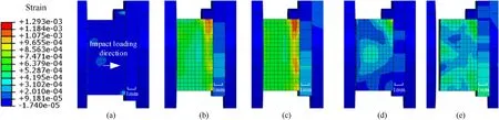
Fig.13.Numerical simulation results of MCT stress nephogram: (a) t = 0 ms; (b) t = 0.5 ms; (c) t = 1.0 ms; (d) t = 1.5 ms; (e) t = 2.0 ms.

Fig.14.The experimental results of DIC strain nephogram: (a) t = 0 ms; (b) t = 0.5 ms; (c) t = 1.0 ms; (d) t = 1.5 ms; (e) t = 2.0 ms.

Table 5 Numerical simulation of peak stress and maximum strain of media in MCT under single pulse stress wave.
The experimental conditions corresponding to each damage mode were numerically simulated.Taking experimental Nos.1, 2 and 5 as examples, the physical mechanism of damage (nonfunctional damage, recovery after transient fault and irreversible functional damage) was studied.Under the finite element simulation of different working conditions,the peak stress and maximum strain of the media in each layer of MCT were shown in Table 5.
(1) Simulation corresponding to experimental No.1
Taking simulation corresponding to experimental No.1 as example,the stress nephogram of the MCT high-voltage switch was shown in Fig.15.It could be seen that there was no large deformation and stress failure zone in each layer of the medium inside MCT, indicating that the device structure of Epoxy resin encapsulation under impact load was complete,which was consistent with the device function under impact load in simulation.
(2) Simulation corresponding to experimental No.2
When the stress wave applied on the specimen for 0.01 ms,dislocations could be observed at the corner of the aluminum 1015 and SiO2contact interface from the stress nephogram,as shown in Fig.16(a).At this point, MCT has been stopped in experiment,multiple capacitors began to charging,the circuit voltage gradually increased to the initial value,and the current also stopped to reduce and gradually increase to the peak.When the stress wave acted on the specimen for 0.08 ms, there was an obvious gap at the corner,and the gap width was 0.11 ms to the maximum value of 0.64 × 10⁻³mm, and then recovered.At the end of the first stress wave, the gap width was fixed at 0.48 × 10⁻³mm, and the stress nephogram was shown in Fig.16(b).The numerical simulation results were consistent with the ultrasonic microscopic scanning results,which proved the effectiveness of the numerical simulation.
Under impact load,the MOSFET structure in MCT was damaged,and there was a gap between the gate of the metal layer and the oxide layer [34,35].When the positive voltage added to the metal gate increased slowly, the majority of carrier holes in the semiconductor were far away from the semiconductor-oxide film interface under the action of Coulomb force, thus forming a depletion layer without carriers.When the voltage further increased and reached a certain value (voltage threshold), the minority carrier electrons in the semiconductor were pulled to the upper part of the depletion layer (near the interface) under the effect of Coulomb force,so an inversion layer with a majority of free electrons was formed near the interface.At this time,the MCT high-voltage switch was on.The impact load results in a gap between the MOSFET metal-oxide layer, so that the oxide insulating layer surface stores enough charge to form an antiform layer,as shown in Fig.17.When the positive voltage was added between the drainsource and the voltage between the gate-source was zero, the charging stored in the metal-oxide layer still caused the current between the drain-source.After a period of time, the elastic deformation stage of the metal layer ended, and the charge between the metal-oxide layer was released.Once again, the MCT high voltage switch was tested and the switch did not appear functional damage.
(3) Simulation corresponding to experimental No.5
The stress nephogram of monocrystalline silicon in MCT highvoltage switch under a single pulse was shown in Fig.18.It could be seen that the stress concentration area appeared at the edge of the monocrystalline silicon inside MCT,and the peak stress reached 40.21 MPa.No obvious gap appeared at the interface between Aluminum 1015 and SiO2in experimental No.3.The failure during this period might be caused by the damage to monocrystalline silicon due to stress concentration.
The monocrystalline silicon was hard and brittle at room temperature, hence it was judged that the failure of monocrystalline silicon in experiment might lead to irreversible functional damage to the specimen.By further refining the grid,the three-dimensional numerical simulation of the crack damage of monocrystalline silicon was carried out.The crack propagation caused by impact load was a complex transient process.The XFEM fracture criterion in ABAQUS software was used to numerically simulate the crack propagation in the internal stress concentration area of the MCT high-voltage switch when the impact velocity was 10.12 m/s [36],As shown in Fig.19,the surface marker close to Epoxy resin was“+”and the surface marker close to Cupronickel was “-”.
The numerical simulation results showed that both the positive and negative sides of the edge of the single crystal silicon had cracks, which was consistent with the crack position obtained by ultrasonic microscopic scanning technology.The reliability of the model used to verify the failure of the device was further verified.The red arrow direction in the figure was the crack extension direction.It could be seen from the figure that when the stress wave lasted for 0.04 ms,the crack began to appear on the“+”surface,and when the stress wave lasted for 0.08 ms,the crack began to appear on the “-” surface, and then the crack gradually extended to the center of the single-crystal silicon.At the moment of 0.20 ms, the cracks on both sides of the single crystal silicon stopped at the same time, and the crack lengths were 0.054 mm and 0.0134 mm,respectively.Due to the energy consumption generated by cracks,the stress in the crack area was less than that in other locations.The formation and propagation of cracks were the result of the combining action of longitudinal compressive stress and transverse stress.When the stress wave propagated along the longitudinal direction of the material, the internal structure of the material led to uneven stress distribution.At the same time, because the crack propagation paths and directions of “+” and “-” surfaces were completely different,the crack of the“-”surface had two turns and the crack length was less than that of the “+” surface, which was caused by the difference in wave impedance of the medium and the uneven stress distribution.When the stress wave reached the “+”plane,the wave impedance of the single crystal silicon was greater than that of the oxide layer.The shock wave was transmitted and reflected.The reflected shock wave collided with the incident shock wave to further raise the stress value of the interface until it met the unloading part of the initial stress wave.When the transmitted wave reached the“-”plane,the shock wave would be reflected and transmitted at the interface because the wave impedance of monocrystalline silicon was less than that of Cupronickel.The reflected shock wave collided with the incident shock wave to further increase the peak stress of the interface.

Fig.16.Stress nephogram of MCT chip (Aluminum 1015, SiO2 and Si): (a) t = 0.01 ms; (b) t = 0.05 ms; (c) t = 0.10 ms; (d) t = 0.15 ms.
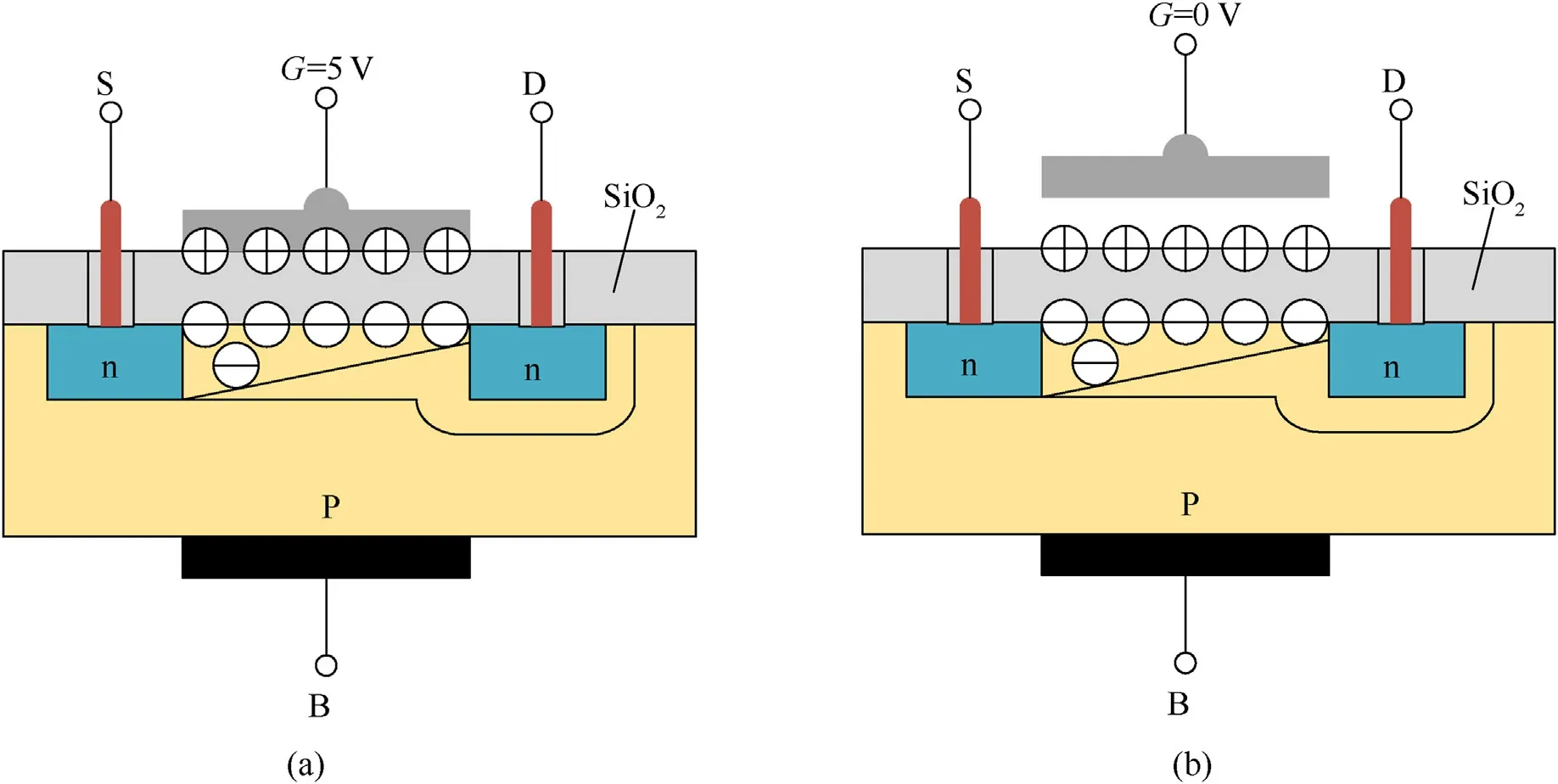
Fig.17.MOSFET conduction principle diagram before and after impact: (a) Before impact; (b) After impact.

Fig.18.Stress nephogram of MCT chip (Aluminum 1015, SiO2 and Si) under single pulse: (a) t = 0 ms; (b) t = 0.05 ms; (c) t = 0.10 ms; (d) t = 0.15 ms.
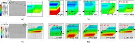
Fig.19.Crack propagation of monocrystalline silicon: (a) “+” crack detail diagram; (b) Crack Propagation on “+”Surface; (c) Details of “-”surface cracks; (d) “-” surface crack propagation.
3.3.Theoretical analysis of stress waves propagation at multilayer interface
The theoretical calculation of stress propagation in the multilayer medium under impact load was very complex.In the experiment, the structure of the MCT high-voltage switch was complex and there were many interfaces.It was difficult to accurately calculate the impact pressure at each interface of the MCT highvoltage switch.To analyze the propagation law of stress waves,the composite structure was simplified as a simple sandwich model.Without considering the transverse effect of stress waves,only the elastic wave generated by collision was quantitatively calculated.Fig.20 listed the stress wave diagram under impact load when the bullet velocity was 7.67 m/s.
In the diagram, only the reflected and transmitted waves generated by the head wave and its arrival at the interface were given, where the “yellow arrow” was the wave head and its transmitted and reflected waves in each layer of medium, and the“green arrow”was the wave tail and its transmission and reflection in each layer of medium.The abscissa was the displacement, and the ordinate was the time, where t1was the duration of the head wave pulse.The stress wave velocity D of each layer of the medium in the Lagrange coordinate system was calculated and substituted into θ = arctan(1/D).The angle between the incident wave, the reflected wave and the transmitted wave, and the x-axis were obtained by calculation, as shown in Table 6.

Table 6 Wave velocity of SHPB system and MCT layers under head wave stress pulse.
When the bullet stroke the incident bar at the contact interface,the stress wave reflected and transmitted at the contact interface between the bullet and the incident bar, and the velocity of the incident bar was [37].
In Eq.(11), ρ0was the bullet density, D0was the elastic wave velocity in the bullet,V0was the initial velocity of the bullet,ρ1was the density of the incident bar, D1was the elastic wave velocity in the incident bar,V1was the initial velocity of the incident bar,and v1was the particle velocity of the incident bar after impact.
The transmitted wave generated by the interface between the bullet and the incident bar propagated along the axis of the incident bar to the MCT.The structure of device was composed of multi-layer media, and the impact impedance of each layer was different.When the shock wave propagated from the medium A with low impact impedance to the medium B with high impact impedance (e.g: from the medium Epoxy resin to the medium Aluminum 1015),the instantaneous reflected wave at the interface should be the loading shock wave in the opposite direction,and the transmitted wave was also the loading shock wave but its direction was the same as the incident shock wave.The Hugoniot equation of the reflected shock wave in the medium A was
In Eq.(12),pAwas the pressure of reflected shock wave in medium A, the density of ρAin medium A, CAwas the sound velocity of medium A, the experimental parameters of SAmaterial, v was the particle velocity at the interface, and vAwas the initial velocity of medium A.The Hugoniot equation of transmitted shock wavefront in medium B was
In Eq.(13),pBwas the pressure of reflected shock wave in medium B, the density of ρBin medium B, CBwas the sound velocity of medium B, and the experimental parameters of SBmaterial.
According to the continuity condition and pressure balance,the particle velocity and pressure behind the reflected wave A should be equal to the particle velocity and pressure behind the transmitted wave array B, respectively.

Then,the rationality of its root was analyzed to determine the final particle velocity, and the corresponding pressure value was obtained through Eq.(13).
When the shock wave propagated from the medium E with high impact impedance to the medium F with low impact impedance in close contact, (e.g: the stress wave propagates from the medium Aluminum 1015 to the medium SiO2), the instantaneous reflected wave on the interface should be the unloading sparse wave with opposite directions, and the transmitted wave was the loading shock wave with the same direction.Similarly, according to the continuous conditions and pressure balance, the particle velocity and pressure in E behind the reflection wave should be equal to those in the medium F behind the transmitted shock wavefront,hence the equations can be solved as follows:
In Eq.(18),pEwas the pressure of reflected shock wave in medium E,the density of medium E in ρE,CEwas the material sound velocity of medium E,the experimental parameters of SEmaterial,v was the particle velocity at the interface, vFwas the initial velocity of medium F, pFwas the pressure of reflected shock wave in medium F,the density of medium F in ρF,CFwas the material sound velocity of medium F, and the experimental parameters of SFmaterial.
The solution can be expressed as
The final particle velocity was determined by the equation and the corresponding pressure value can be obtained by Eq.(19).
Based on the above calculated method, the electrical output parameters of the MTC high-voltage switch under impact load are not affected, and the recovery and irreversible functional damage after transient fault were theoretically deduced, and the results could be compared with those obtained by numerical simulation[38].As shown in Fig.21,the interface between the incident bar and Epoxy resin was defined as “1”, the interface between Epoxy resin and Aluminum 1015 was “2”, the interface between Aluminum 1015 and SiO2was “3”, and the interface between SiO2and Si was“4”.The interface between Si and Cu was “5”, and the interface between Cu and PCB was “6”.
The attenuation of stress waves could not be simply regarded as the interaction between the front shock wave series and the interface.This interaction was completely determined by the scale of shock overload, which depended on the relative thickness of each layer in the multilayer structure and the relationship between them and the initial pulse width.In theoretical derivation, the model structure was simplified as a“sandwich”structure,ignoring the influence of wiring, solder joints and other factors on the specimen.The results of numerical simulation were compared with the theoretical derivation and numerical simulation by collecting the average stress between layers.The error of the interface on both sides of Epoxy resin was the largest.The reason was that it was not a regular shape with the encapsulation of Epoxy resin, and its encapsulation structure was semi-encapsulated on the internal chip structure.The sandwich model could not accurately calculate it.When it reached Aluminum 1015, the error at the interface between SiO2and Si was significantly reduced, and the “sandwich”-model could well express the interface stress.There was also a certain error at the interface between Si and Cupronickel, which might be related to the uneven and irregular shape of solder joints on Cupronickel, production process, assembly process and other factors.

Fig.21.Comparison of theoretical calculation and numerical simulation: (a) Electrical output parameters have no effect; (b) Recovery after transient fault; (c) Unrecoverable functional damage.
4.Conclusions
In this paper,experiments,numerical simulation and theoretical analysis are combined to study the electro-mechanical coupling response characteristics of MCT high-voltage switch under impact load.The damage modes of MCT high-voltage switch under impact load are divided into non-functional damage, recoverable functional damage, non-recoverable damage and structural damage.The following conclusions could be drawn:
(1) When the overall strain is less than or equal to 0.026,and the peak stress is less than or equal to 10.55 MPa,it has no effect on the function of the device,that is,non-functional damage.When the overall strain is in the range of 0.045-0.046 and the peak stress is in the range of 41.70-46.70 MPa, the functional damage occurs.After the device is left for 5 min,the function will return to normal, that is, the functional damage can be recovered.When the global strain ranges from 0.046 to 0.052,and the peak stress ranges from 51.98 to 53.48 MPa, the functional damage occurs, which does not recover after standing, that is, the functional unrecoverable damage.When the bullet velocity was 25.61 m/s, the MCT's epoxy encapsulation was crushed.
(2) The mechanical response of MCT high voltage switch under different impact loads is analyzed by numerical simulation,and the accuracy of numerical simulation is verified by DIC technology.The failure mechanism of functional recovery damage can be attributed to the situation that the insulating oxide layer is charged due to the gap between the metal gate and the oxide layer in the internal MOSFET structure,which leads to the failure of the device.After a period of time, the elastic deformation of the metal gate recovers, the accumulated charge disappears, and the device can return to the normal working state.Obvious cracks appears on both sides of the monocrystalline silicon in the MCT high-voltage switch during loading, which is the fundamental cause of irreversible functional damage of the device.
Declaration of competing interest
The authors declare that they have no known competing financial interests or personal relationships that could have appeared to influence the work reported in this paper.
Acknowledgements
The research was supported by Youth Talent Project of Basic Scientific Research Project of Liaoning Province Education Department (Grant No.LJKZ0270), Youth Project of Basic Scientific Research Project of Liaoning Province Education Department(Grant No.LJKQZ2021055).

- Defence Technology的其它文章
- Ground threat prediction-based path planning of unmanned autonomous helicopter using hybrid enhanced artificial bee colony algorithm
- Layered metastructure containing freely-designed local resonators for wave attenuation
- Predicting impact strength of perforated targets using artificial neural networks trained on FEM-generated datasets
- Construct a 3D microsphere of HMX/B/Al/PTFE to obtain the high energy and combustion reactivity
- Ignition processes and characteristics of charring conductive polymers with a cavity geometry in precombustion chamber for applications in micro/nano satellite hybrid rocket motors
- Recent research in mechanical properties of geopolymer-based ultrahigh-performance concrete: A review