
Cathodic shift of onset potential on TiO2 nanorod arrays with significantly enhanced visible light photoactivity via nitrogen/cobalt co-implantation*
2021-05-24 02:22XianyinSong宋先印HongtaoZhou周洪濤andChangzhongJiang蔣昌忠
Chinese Physics B 2021年5期
Xianyin Song(宋先印), Hongtao Zhou(周洪濤), and Changzhong Jiang(蔣昌忠)
College of Materials Science and Engineering,Hunan University,Changsha 410082,China
Keywords: ion implantation,TiO2,surface sputtering,photo-electrochemical water splitting
1. Introduction
Since Fujishima and Honda reported the photo-oxidation of water on TiO2in 1972,[1]TiO2has been extensively investigated as a photoanode material due to its high water-oxidation activity, excellent photostability, and earth abundance.[2–4]However, the poor visible light photo-activity induced by its wide band gap (Eg=3.0 eV) is the major limitation for its further application as photo-anode.[5]Although anionic doping(e.g., N,S)could effectively increase the visible-light response of TiO2, it also causes a significant anodic shift in current onset potential.[6–8]And this can be ascribed to the introduced impurity states above the valence band maximum(VBM)and large number of surface lattice defects,which decrease the oxidative capability and surface transfer dynamics of photo-generated holes.[9,10]Meanwhile,the onset potential of photo-anodes plays a critical role in building highly efficient and unassisted hetero-type PEC water-splitting cells.[11–13]
To reduce the onset potential, the most commonly used method is loading various oxygen evolution catalysts on anion-doped TiO2.[8,14]This method could efficiently decrease onset potential;however,the loaded electrocatalyst layers were easy to fall off and even affected the light-harvesting of the underneath semiconductor. Besides,Jang et al.reported another re-growth strategy to reduce structural disorders at the surface of photoanodes and had achieved cathodic shift in turn-on voltage.[11]However,this method is uncontrollable.Therefore,a general approach with high controllability is still desired.
Ion implantation, a typical surface engineering technology,has been widely used to tailor the electronic properties of semiconductor in industry.[15]It is a general method for introducing different and/or multiple elements of interest into semiconductor for systematic studies.[7]The implanted ions are presented in a highly dispersed state in the TiO2lattice.[10,16]Meanwhile,as a compulsive doping approach,high-energy ion bombardment could not only produce lattice defects,but also induce surface sputtering effect.[17–19]
Herein, considering the high controllability at impurity distribution and surface sputtering effect of ion implantation technology,[16,20]we used ion-implantation approach to codope nitrogen and cobalt into TiO2nanorods for PEC water oxidation (Fig. 1(a)). Our results demonstrate that the surface lattice disorder of N-TiO2can be effectively removed by surface synergic sputtering of nitrogen/cobalt ions. And the surface synergic sputtering endows a cathodic shift of 350 mV in onset potential and more than 6.5 times increase of visible light photo-activity for N/Co-TiO2samples, relative to only nitrogen doping (N-TiO2). Our results demonstrated ion implantation was a novel and useful strategy for cathodic shift of TiO2photo-anode with improved catalytic activity.
2. Methods
2.1. Sample preparation
The TiO2nanorod array was grown on FTO glass via a well-developed hydrothermal method.[21]The obtained TiO2nanorod arrays were then annealed at temperature 550°C for 3 hours in air. The nitrogen ions and cobalt ions were coimplanted into the TiO2nanorod array using a Kaufman ion source and a metal vapor vacuum arc (MEVVA) ion source implanter, respectively. The as-implanted TiO2were finally annealed at 550°C for 3 hours in high vacuum(approximately 10?4Pa) (Fig. 1(b)). The nitrogen-doped and cobalt-doped TiO2nanorod arrays were also prepared via ion implantation and subsequent high-vacuum annealing procedures.

Fig.1. (a)Simplified diagram schematic of N/Co ion co-implantation. (b)Schematic diagram of the fabrication process of N/Co-TiO2 by ion implantation method. (c)SRIM calculated concentration profiles of N ions and damage(Ti recoil and O recoil)in TiO2 at the implantation energy of 30 keV to a dose of 3×10¹⁵ ions/cm2. (d)SRIM simulated surface sputtering yield by 30-keV N ions and 119-keV Co ions.
2.2. Photo-electrochemical measurements
Photo-electrochemical (PEC) measurements were performed in a three-electrode cell under a solar simulator(a 500-W xenon lamp coupled with an AM 1.5 G filter) at an illumination intensity of 100 mW/cm2. The TiO2photo-anodes were used as working electrodes, and a Pt foil was used as a counter electrode. An Ag/AgCl(saturated KCl)electrode was served as reference electrodes and 1.0-M NaOH aqueous solution(pH=13.6)was used as the electrolyte. The illuminated area was fixed at 0.785 cm2(a sealing ring with 1 cm in diameter). The measured potentials were converted to reversible hydrogen electrode (RHE) potential according to the Nernst equation

2.3. Material characterization
Scanning electron microscopy(SEM)was performed on a JEOL S-4800 microscope. Transmission electron microscopy(TEM)were carried out on a JEOL JEM2010. X-ray diffraction (XRD) patterns were recorded using a Bruker AXS, D8 Advance x-ray powder diffractometer with Cu-Kα irradiation(wavelength 1.5418 ?A).Raman spectroscopy was collected using a commercial Raman microscope(HR800, Horiba)and a laser emitting at 488 nm was served as the excitation source.X-ray photoelectron spectroscopy (XPS) experiments were done on a Thermo Scientific ESCALAB 250Xi system using Al Kα radiation source of 1486.6 eV,with C 1s(284.8 eV)as calibration reference.
3. Results and discussion
3.1. SRIM simulation
An implanted high-energy ion will lose its energy through a series of cascade collisions with the target atomic nucleus and extranuclear electrons, and its distribution law in the target material is clearly recognized and well determined. We can accurately design the depth distribution of dopant ions in TiO2through adjusting the ion implantation energy.
Besides,the atomic collision can transfer enough energy to target atoms to produce irradiation damage and surface sputtering. Figure 1(c)shows the calculated concentration profiles for implanted N ions,as well as damages(Ti recoil and O recoil)in TiO2according to SRIM simulation. The simulations show the maximum defect damage is much closer to the surface than the maximum N ion location. Meanwhile, the simulated surface sputtering yield of TiO2is shown in Fig. 1(d).Clearly, the sputtering yield induced by 119-keV Co ion is much higher than that of 30-keV N ion. In addition,the sputtering yield of lattice oxygens is more than twice than that of Ti atoms,showing preferential sputtering to oxygen atoms. This is consistent with previous experiment reports.[18,20]
3.2. Structure characterization
Figures 2(a)–2(h) show the SEM images of the original TiO2, N-TiO2, Co-TiO2, and N/Co-TiO2. The pristine TiO2nanorod presents a smooth side face and rectangular cross section with some bumps at the top. And the morphology of N-TiO2and Co-TiO2do not exhibit obvious changes compared to the pristine TiO2. However, the rough cross-section at the top of nanorods becomes smoother for N/Co-TiO2samples (Figs. 2(g)–2(h)). Meanwhile, the N, Co co-implanted TiO2samples without subsequent annealing treatment (asimplanted N/Co-TiO2)have already presented smoother crosssection at the top, as shown in Fig. S1 in Supporting information. It means TiO2nanorod tip can be effectively etched by the synergic sputtering of high-energy nitrogen ions and cobalt ions. It is worth noting that the irradiation damages at the top of TiO2nanorod have been effectively removed at the same time, confirmed by the HRTEM results as shown in Fig. S2. Besides, figures S3(a)–S3(b) also show that the surface etching become more evident as increasing the cobalt ion dose. The surface sputtering yield and ion irradiation induced surface patterns are affected by multiple factors, such as ion species, ion energy, crystal orientation, temperature of substrate materials,etc.[17,19,21]While,it needs to be emphasized that the surface synergic sputtering of N/Co ions is not the simple dose superimposed effect,as these surface etching is obviously different from our previous C/N ion co-implantation and high-dose Cr ion implantation.[10,16]Even though,the inherent mechanism of synergic sputtering by N/Co ions here needs to be further studied.
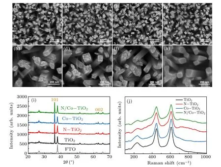
Fig. 2. SEM images of [(a) and (b)] the pristine TiO2, [(c) and (d)] nitrogen-doped TiO2 with a nitrogen dose of 3×10¹⁵ ions/cm2 (N-TiO2), [(e)and (f)] cobalt-doped TiO2 with a cobalt dose of 3×10¹⁵ ions/cm2 (Co-TiO2), [(g) and (h)] nitrogen/cobalt co-doped TiO2 with a nitrogen dose of 3×10¹⁵ ions/cm2 and a cobalt dose of 3×10¹⁵ ions/cm2 (N/Co-TiO2). (i)XRD patterns of FTO,pristine TiO2,N-TiO2,Co-TiO2,and N/Co-TiO2. (j)Raman spectra of pristine TiO2,N-TiO2,Co-TiO2,and N/Co-TiO2.
Figure 2(i) displays the XRD patterns of FTO substrate, pristine TiO2, N-TiO2, Co-TiO2, and N/Co-TiO2. It is indicated that all the samples were rutile phase TiO2[22]and no additional phase was detected after ion implantation and annealing, even for high-dose ion implantation samples(Fig.S3(c)).It further demonstrates that the implanted ions are presented in a highly dispersed state in the TiO2lattice via ionimplantation method. Raman spectroscopy studies also confirmed the conclusion of XRD analysis. There are four typical Raman-active modes with frequencies at 610, 447, 235, and 141 cm?1(Fig.2(j)and Fig.S3(d)),corresponding to the A1g,Eg, multi-photon and B1g modes of the rutile space group(P42/mnm), respectively.[23]However, it is also noteworthy that some new modes emerge at the range from 700 cm?1to 900 cm?1for nitrogen-doped TiO2, suggesting structural changes occurred after doping.[2]
3.3. Photo-electrochemical measurement
PEC performances were investigated under a simulated solar irradiation of 100 mW/cm2with or without through a visible-light cutoff filter of 420 nm. Figure 3(a) shows the linear sweep voltammogram collected for pristine TiO2, NTiO2, and N/Co-TiO2under dark and AM 1.5 G irradiation.Compared to the pristine TiO2, the N-TiO2sample exhibits an enhanced photocurrent density under high-bias voltages(>1.6 V versus RHE), but nearly 0.6-V anodic shift in current onset potential is observed,which directly leads to a much lower photocurrent density(0.17 mA/cm2)at the typical voltage of 1.23 V versus RHE.However,as the Co ions was subsequently implanted into N doped TiO2,the photocurrent density of N/Co-TiO2sample reaches 0.73 mA/cm2at 1.23 V versus RHE under simulated solar irradiation, which is more than twice higher than that of the pristine TiO2(0.33 mA/cm2)obtained at the same potential. Most importantly, relative to the negligible visible-light response of pristine TiO2as expected, the N/Co-TiO2sample showed a significant cathodic shift of 350 mV in onset potential and more than 6.5 times increase of visible-light catalytic activity than that of N-TiO2(0.46 mA/cm2versus 0.07 mA/cm2at 1.23 V versus RHE)(Fig. 3(b)). In addition, the visible-light PEC activity of Co-TiO2was also studied. Figure S4 in Supporting information shows the increase of visible-light catalytic activity for Co-TiO2is slight and negligible.
The dosage effects of N/Co ions on PEC performance were also studied (Fig. 3(c)). The optimized PEC performance for N/Co co-implanted TiO2was obtained with an implantation ion fluence of 3×10¹⁵ions/cm2nitrogen and 3×10¹⁵ions/cm2cobalt. Further increase of cobalt implantation dose can induce a decrease in photo-activity. The excessive Co ion implantation could produce other irreparable surface lattice damages that also can act as the recombination centers to degrade the overall photo-activity,despite high-dose Co doped TiO2(Co+-TiO2)shows enhanced visible-light catalytic activity(see Fig.S5).

Fig.3. (a)Linear sweep voltammetry of TiO2,N-TiO2,and N/Co-TiO2 under AM 1.5 G irradiation. (b)Linear sweep voltammetry of TiO2,N-TiO2,and N/Co-TiO2 under visible light irradiation. (c) The histograms of AM 1.5 G and visible-light photocurrent density for N/Co co-doped TiO2 with different cobalt doses to the same nitrogen dose of 3×10¹⁵ ions/cm2.
3.4. Chemical state analysis
XPS measurements were carried out to further investigate the chemical states of N and Co atoms in TiO2, particularly for N-TiO2and N/Co-TiO2samples. The survey spectrum of N/Co-TiO2sample shows the presence of weak N and Co signals (Fig. S6(a)), and the carbon signals were used for calibration of the binding energy(Fig.S6(b)). Figure 4(a)shows N 1s spectra of N-TiO2and N/Co-TiO2samples. There are several broad peaks from 394 eV to 404 eV,which can be deconvolved into three peaks located at around 402, 400, and 396 eV corresponding to the chemical bonding of N–N,N–O,and N-Ti bonds, respectively.[7,8]Between them, the substitution N-Ti states are mainly responsible for the visible light absorption according to previous theoretical and experimental evidences.[8,24,25]A negative shift (~0.26 eV) of N-Ti peak can be observed in N/Co-TiO2samples, suggesting the increasing electron density around N atoms. However,this shift cannot be ascribed to the N–Co interaction,because the binding energy of N–Co is stronger than N-Ti bonding.[8,26]
Figure 4(b) shows the XPS Co 2p spectra of Co-TiO2and N/Co-TiO2. Two peaks centered at 781 eV and 796.5 eV are observed, which can be assigned to Co 2p3/2and Co 2p1/2of Co2+in TiO2, respectively.[27,28]And it can be seen that two satellite peaks located at approximately 786.6 eV and 802.8 eV appeared, which also can be ascribed to Co2+species,[27]consistent with the literature values of Co-doped TiO2.[29,30]Impressively, the Co 2p spectrum of N/Co-TiO2also exhibits a negative shift in binding energy. Meanwhile,similar shift to lower energy region for N/Co-TiO2samples is also observed in XPS Ti 2p and O 1s spectra, compared to N-TiO2as shown in Figs. 4(c)–4(d). The negative shift in XPS spectra of N/Co-TiO2can be ascribed to the excess electrons from oxygen vacancies transferring to other atoms. And the more oxygen vacancies incorporated into N/Co-TiO2can arise from the preferential sputtering of lattice oxygen in TiO2by high-energy N/Co ions,which has confirmed in Figs.1(d)and 2(g)–2(h).
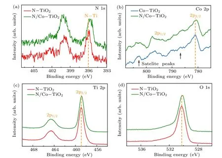
Fig.4. (a)XPS N 1s spectra of N-TiO2 and N/Co-TiO2,(b)XPS Co 2p spectra of Co-TiO2 and N/Co-TiO2,(c)XPS Ti 2p spectra,and(d)O 1s spectra of N-TiO2 and N/Co-TiO2.
3.5. Electrochemical characterization
To further clarify the intrinsic electronic properties of N-TiO2and N/Co-TiO2, we have performed electrochemical impedance investigations. The Mott–Schottky plots was used to calculate the carrier densities and flat band potential at the electrode/electrolyte interface according to the equations given below:
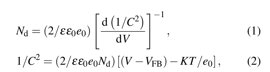
where ε is the dielectric constant of rutile TiO2(ε =170),[5]ε0is the permittivity of vacuum, e0is the electron charge,V is the applied potential, C is the capacitance between TiO2and electrolyte(in units of F·cm?2), Ndis the carrier density,VFBis the flat band potential, K is the Boltzmann constant,and T is the absolute temperature (in unit K). In Fig. 5(a)and Fig. S7, the positive slope of Mott–Schottky plots indicates the n-type semiconductor characteristics. Obviously,the N/Co-TiO2exhibits a smaller slope than TiO2and NTiO2, indicating a much higher donor density. The carrier densities of TiO2, N-TiO2, and N/Co-TiO2calculated from Eq. (1) are 1.88×10¹⁷, 1.21×10²¹, and 2.43×1021cm?3, respectively. The increased donor concentration of N/Co-TiO2is mainly attributed to the incorporated oxygen vacancies by high-vacuum annealing and preferential sputtering of lattice oxygen. And these oxygen vacancies could serve as electron donors in TiO2[5,7]and enhance the charge separation efficiency from bulk to surface.[7,8]
However, large numbers of surface and bulk defects are also introduced during the ion implantation. Although partial of lattice defects have been repaired after subsequent heat treatments, many defects still survived at the surface of Ndoped TiO2(Fig. S2(b)), especially under high-dose ion implantation. These surface lattice disorders act as deep energy level, which can result in Fermi level pinning and a significant anodic shift of the flat band potential (VFB).[11,20,31]Fortunately, these surface defects have been effectively removed through the surface synergic sputtering induced by high-energy N/Co ions (Fig. S2). Therefore, the N/Co-TiO2sample displays a huge cathodic shift of VFBand onset potential,relative to the N-TiO2(Figs.5(a)and 3(a)).

Fig. 5. (a) Mott–Schottky curves for N-TiO2 and N/Co-TiO2 samples collected at the frequency of 1 kHz in dark. (b) Nyquist plots obtained at a potential of 1.23 V(versus RHE)under AM 1.5G irradiation.
Finally, we will further investigate the charge transfer properties at the TiO2/electrolyte interfaces for N-TiO2and N/Co-TiO2through the electrochemical impedance spectroscopy(EIS).Figures 5(b)and S8 show the Nyquist plots of N-TiO2and N/Co-TiO2acquired from EIS measurements. All the Nyquist plots exhibited semi-circles and the data were well fitted by a typical Randles circuit model (insets, Fig. 5(b)),which consisted of the total series resistance (RS), constant phase angle element (CPECT), and charge-transfer resistance(RCT)at the TiO2/electrolyte interfaces.[7,32]The fitted charge transfer resistance (RCT) for N/Co-TiO2was less than half than that of N-TiO2(detailed values, see Table S1), indicating superior charge transfer kinetics of photo-generated carriers at the electrode/electrolyte interface for N/Co co-implanted TiO2. As a consequence, the N/Co-TiO2samples show obviously increased PEC performances, compared to the N-TiO2(Fig.3).
4. Conclusion
In summary, we have successfully achieved a huge cathodic shift in onset potential for TiO2photo-anode with significantly enhanced visible light photo-electrochemical performances through N/Co co-implantation. Due to the synergic sputtering of implanted N/Co ions,the surface lattice disorder induced by ion bombardment has been effectively removed.As a consequence,the N/Co co-implanted TiO2exhibits a cathodic shift of 350 mV in onset potential and more than 6.5 times increase of visible-light photocurrent density at 1.23 V versus RHE relative to only N-implanted TiO2. Our work demonstrates that ion implantation technology is a powerful method to modulate the band structure of photo-electrodes,and thus improve their PEC performances. We believe ion implantation is a general strategy which can be extended to introduce different dopants into different semiconductor materials for PEC water splitting and possibly other applications such as solar cells and photodetectors.
- Chinese Physics B的其它文章
- Corrosion behavior of high-level waste container materials Ti and Ti–Pd alloy under long-term gamma irradiation in Beishan groundwater*
- Degradation of β-Ga2O3 Schottky barrier diode under swift heavy ion irradiation*
- Influence of temperature and alloying elements on the threshold displacement energies in concentrated Ni–Fe–Cr alloys*
- Review on ionization and quenching mechanisms of Trichel pulse*
- Thermally induced band hybridization in bilayer-bilayer MoS2/WS2 heterostructure?
- Universal memory based on phase-change materials: From phase-change random access memory to optoelectronic hybrid storage*