
Universal memory based on phase-change materials: From phase-change random access memory to optoelectronic hybrid storage*
2021-05-24 02:22BoLiu劉波TaoWei魏濤JingHu胡敬WanfeiLi李宛飛YunLing凌云QianqianLiu劉倩倩MiaoCheng程淼andZhitangSong宋志棠
Chinese Physics B 2021年5期
Bo Liu(劉波), Tao Wei(魏濤), Jing Hu(胡敬), Wanfei Li(李宛飛),Yun Ling(凌云), Qianqian Liu(劉倩倩), Miao Cheng(程淼), and Zhitang Song(宋志棠)
1Research Center for
Nanophotonic and Nanoelectronic Materials,School of Materials Science and Engineering,
Suzhou University of Science and Technology,Suzhou 215009,China
2State Key Laboratory of Functional Materials for Informatics,Shanghai Institute of Microsystem and Information Technology,Chinese Academy of Sciences,Shanghai 200050,China
Keywords: universal memory, optoelectronic hybrid storage, phase-change material, phase-change random access memory
1. Introduction
With high-definition video and intelligent electronic products entering our life,we are gradually entering the era of information explosion.The volume of digital information generated from the internet and from portable and high-definition video devices has doubled every two years since 2000 and will reach 44 zettabytes(or 44 billion terabytes (TB))by 2020.[1]In addition,with the technology upgrading and application of mobile Internet, cloud/sea/fog computing, Internet of things,artificial intelligence, smart city, and smart earth, the global data will grow exponentially. The value of big data has received more and more attention. Hence,information will need to be continuously stored and readily accessed over long-term periods. These stringent requirements constitute an insuperable challenge for existing data centers. The current data storage mode is divided into cold storage and hot storage. The cold storage is mainly used to store large-scale data that is not often used, such as library books, hospital imaging, meteorological information,and other social data. While the hot storage is mainly used to store frequently used data, such as consumer electronics and data center information. At present,cold storage mainly uses magnetic hard-disk, tape and optical disk as storage medium, while hot storage basically uses semiconductor memory, such as DRAM and FLASH. The hardware platform based on von Neumann computing architecture needs a large amount of data to be transmitted frequently between processing (central processing unit, CPU)and memory (SRAM/DRAM with high speed but volatility and FLASH/hard-disk with low speed but non-volatility)units.[2]While in memory units, frequently accessed data are loaded temporarily in SRAM/DRAM and the remaining data are kept in FLASH/hard-disk for long-term storage. Therefore, the shuffling of data between these units exposes the shortcomings of”memory bottleneck”. The disadvantages of memory and computing separation are more prominent when it comes to big data computing. Nonvolatile memristor can realize data storage and in-memory computing at the same time, that is, the integration of storage and calculation can eliminate the memory bottleneck fundamentally. At present,nonvolatile memristors mainly include phase-change random access memory(PCRAM),ferroelectric random access memory(FeRAM),resistive random access memory(RRAM),and magnetoresistive random access memory(MRAM),etc.[3–15]The comparison of physical performance for PCRAM with other nonvolatile devices,such as FLASH,FeRAM,MRAM,and RRAM has been reported in Ref.[14].
Among emerging nonvolatile memory devices, PCRAM is the most mature and has been considered to be one of the most promising candidates for next-generation nonvolatile memory. The physical basis for PCRAM is the phase change of chalcogenide alloy. The development history of phasechange materials and some important events in their applications are shown in Fig.1.

Fig.1. The development history of phase-change materials and some important events in their applications.
The first observation of phase change induced by electrical current was reported in MoS2.[16]Ovshinsky first developed both electrically controlled threshold and memory switching devices[17]and laser-induced phase change for amorphous chalcogenide films.[18]Two of the most important phase-change materials, which are GeSbTe and AgInSbTe, were discovered in 1987 and 1991 respectively. The reversible reflectivity change in the chalcogenide alloy film has been firstly applied in phase-change rewritable optical disk successfully since 1990s. This technology became the mainstream in optical disk and resulted in the commercialization of 650-MB compact disk rewritable (CD-RW), 4.7-GB digital versatile disk rewritable (DVD±RW) or digital versatile disk random access memory(DVD-RAM),and 20 GB–27 GB high-density digital versatile disk(HD-DVD)or blue-ray disk(BD).[19,20]The establishment of Ovonyx in 1999 marks the formal rapid development of PCRAM. After ten years of research and development,PCRAM has finally entered the stage of industrialization. In 2010,the commercial availability of a 512-Mb PCRAM die(labeled as KPS1N15EZA)inside a mobile handset has been confirmed by UBM TechInsights.[21]On 28 July 2015, 3D XPoint named as Optane memory, which consists of 3D crossbar array structure with a selector and a memory cell both based on phase-change materials, has been announced by Intel and Micron[22]and has entered the market as Optane solid-state drive (SSD)[23]and storage class memory(SCM).[24,25]In 2018,Intel announced a new class of Optane memory named as Optane DC Persistent Memory, with capabilities that would bridge the gap between SRAM/DRAM and non-volatile storage while expanding the amount of memory available per CPU socket to as much as 3 TB.[26]If Optane DC Persistent Memory is integrated with DRAM,the computing efficiency of big data centers and large servers will be improved by about two orders of magnitude.[26]However, it is difficult to replace existing mature memory technologies because the programming speed of this device is slightly slower than that of DRAM although it has a larger storage capability and nonvolatile features. Some improvements on performance of PCRAM in terms of access time, storage density, power consumptions, reliability, and price point are still being pursued. In order to further improve the storage performance of PCRAM,many new storage concepts based on phase-change materials will appear in the future. For example, applying different optical/electrical pulses can obtain continuous resistance changes and the output of multiple phase-change neurons will be slightly different even using the same input signal,which is the characteristics of biological neurons. This characteristic makes it have broad commercial prospects in neuroinspired computing, which has gradually become a research hotspot. In this paper, the research progress of phase-change materials and device structures for PCRAM, as well as the most critical performances for a universal memory, such as speed,capacity,and power consumption,are reviewed and the new concept of optoelectronic hybrid storage based on phasechange material is proposed and its feasibility to replace existing memory technologies as a universal memory is also discussed.
2. Principles of PCRAM
In phase-change memory studies, the programming of information bits is accomplished by means of thermally/optically/electrically induced phase changes between the amorphous and crystalline states in phase-change material film as shown in Fig. 2.[27]The reversible structural change in the films results in a pronounced change of material reflectivity and resistivity, which can be measured in the information readout operation. An initially amorphous as-deposited phase-change layer is crystallized by exposure to a laser beam or an electrical pulse with intensity sufficient to heat the material to a temperature above the glass-transition temperature,which is called SET process. By using a short laser or electrical pulse with high intensity enough to melt the phase-change layer can then convert the crystalline phase into the amorphous one after quenching. The reversible resistivity change in the alloy film can be applied in a new non-volatile memory named as PCRAM, which has been pursued for many years.The early work disclosed some of the fundamental concepts of the PCRAM,such as storage materials, storage principles,device structures and prototype devices. It is only in the past 15 years that advances in materials and device technology have made it possible for PCRAM to be one of the most competitive new storage technology to replace incumbent mainstream technologies such as FLASH and DRAM,where the computing and storage memories could be unified.[28–31]
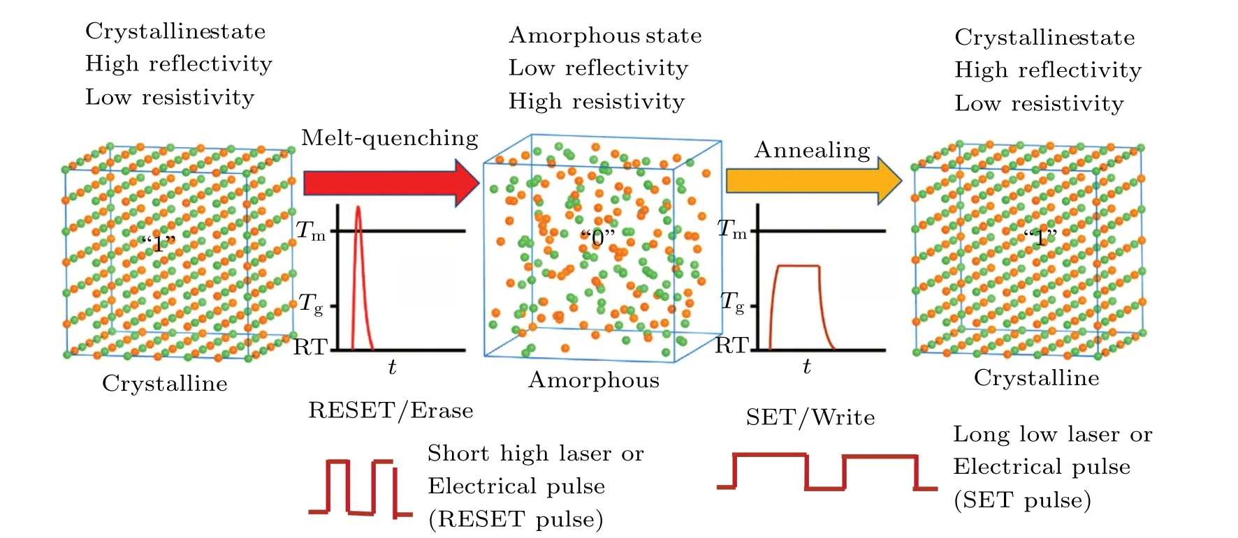
Fig.2.Models of amorphous and crystalline phase-change materials.In phase-change material memory devices,the amorphous and crystalline states are used to encode information. Large contrast in reflectivity or resistivity between the amorphous and crystalline phases of phase-change materials defines the two logic state as“0”and“1”. Fast and reversible switching between the two states is achieved by crystallization(SET/Write)and amorphization(RESET/Erase). Reproduced with permission.[27] Copyright 2019,WILEY-VCH Verlag GmbH&Co. KGaA.
3. Comprehensive performance optimization of PCRAM
In order to replace existing memory technologies,such as SRAM, DRAM, and FLASH, and become a universal memory, performance of PCRAM in terms of access time, storage density,power consumption,and reliability should be improved greatly. According to the general heat formula as shown in Fig. 3, the power consumption of PCRAM device cell is related to many factors, such as operating current,phase-change material characteristics,device structure,heater materials, chip circuit design, etc. In PCRAM device cell,the reversible phase-change resistor plays a dual role, which is to consume heat inducing phase transition between amorphous and crystalline states, and generate heat due to its resistance characteristic. For the latter, in order to improve the heat production capacity of reversible phase-change resistor,it is necessary to increase operating current I, phase-change time t, and resistivity ρ. However, increasing the operating current and the phase-change time are not the best choice for low power consumption and high speed. It is feasible to increase the resistivity in a reasonable range, which can be realized by doping phase-change materials (see Section 4) and introducing buffer-layer between phase-change materials and heater electrode. For the former,in order to obtain low power consumption, the following factors need to be considered at least:low operating current,small phase-change volume,high speed,and high heating efficiency,etc.
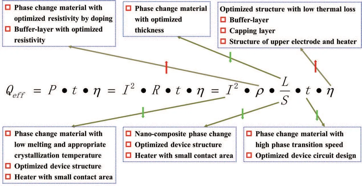
Fig.3. Heat consumption affecting factors of PCRAM device cell. Here,Qeff is defined as the effective heat for phase-change process,P is the power,t is the phase-change time,η is heating efficiency,I is the operating current,R is the resistance of PCRAM cell,ρ is the resistivity of PCRAM cell,L is the thickness of phase-change material,S is the phase-change area contacting with the heater. The red up arrow represents increasing and the green down arrow represents decreasing. The contents in the dotted box represent the corresponding improvement methods.
3.1. Low operating current
The large programming current is still one of the most important issues that limit the adoption of PCRAM in many applications, especially in the field of consumer electronics, SCM, and brain like computing. Furthermore, excessive operation current also restricts the further improvement of PCRAM integration. Therefore, reducing the programming current (particularly RESET current due to the melting of phase-change material)is necessary for achieving both high-density and low power consumption of PCRAM. In a PCRAM cell, the RESET current is affected, at least, by the device structure/size and the phase-change materials properties, such as melting temperature, electrical resistivity, thermal conductivity, composition of the chalcogenide film, and the degree of crystallization, which changes according to the setting time of phase-change material, the electrical resistivity and thermal conductivity of top/bottom electrode, dielectric environment, and device circuit design.[32]It was shown that the main source of heat for amorphization is the phasechange material bulk and interface regions instead of the contacting electrode.[33]Therefore, a phase-change layer with a much higher resistivity, which can be realized by doping or disorder,[34,35]than the resistive heater is necessarily adopted for a higher energy efficiency to markedly reduce RESET current.[36]The bottom electrode(BE)named as heater plays a dual role, that is a current supplier and a “cooler” (as opposed to the heater) to insulate the phase-change area from a thermal sink. A small-contact-area heater is used primarily to minimize heat loss from the phase-change layer and therefore is one of the most important key processes to reduce the operating current. Figure 4 shows the RESET current and current density as a function of the equivalent diameter of a circular contact.[3,32,37–47]It is very clear that the RESET current scales with the effective contact area of the PCRAM and normally the minimum current density of 10 MA/cm2may be required even with carefully engineered cell structures and materials.[3]The RESET current for a 45-nm 1-Gb chip with a self-aligned μTrench-based cell architecture is 200 μA.[48]By using thermally confined TaN/TiN BE, the RESET current is 30 μA with BE diameter of 39 nm, which represents a 90% reduction compared with conventional solid TiN.[38]Charge-injection GeTe/Sb2Te3superlattice PCRAM with the BE with diameter of 50 nm can operate with a RESET-current of 70μA and a SET-speed of 10 ns.[41]Based on confined cell structure and novel BE materials with 7.5 nm×22 nm contact area, the fully integrated 20-nm node size PCRAM device was successfully produced and the RESET current was below 100 μA.[37]PCRAM cells with single-wall and smalldiameter multi-wall carbon nanotube electrode achieve RESET current of 5μA/1.4μA for carbon nanotube diameter of 5 nm/1.2 nm.[39,40]In addition to reducing the heater contact diameter, other methods can also effectively reduce the RESET current,even less than current density of 10 MA/cm2. By using a low current SET pre-operation method:the low sweeping current induces Ge2Sb2Te5(GST)into the crystalline state with high degree of disorder to facilitate the amorphization,the RESET current density is only 4.84 MA/cm2,which is possible to integrate a selector in the same scale for 3D cross-point applications.[46]Unlike the melt-quench strategy to induce amorphization,introducing defects in the crystalline phase can engineer carrier localization effects enhancing carrier–lattice coupling; and this can efficiently extract work required to introduce bond distortions necessary for amorphization without an intermediate melting process from input electrical energy, which shows tremendous improvement in RESET current densities by two orders of magnitude[49]and current density as low as ~0.3 MA/cm2are achieved for Bi-doped GeTe nanowires.[47]
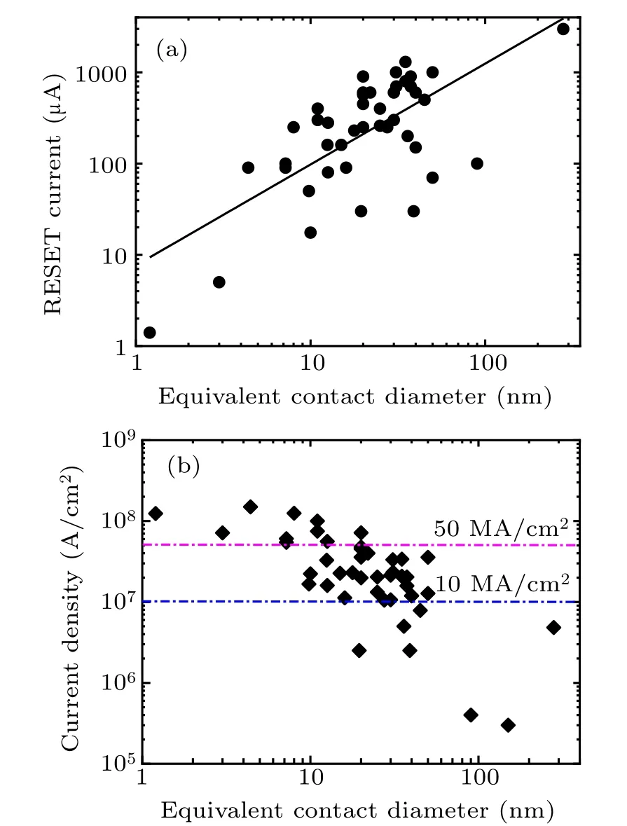
Fig.4. RESET current(a)and current density(b)as a function of equivalent contact diameter,showing a linear scaling trend of RESET current with the effective contact area as the device feature size goes down.
3.2. Small phase-change volume
Obviously, when the volume involved in the phase transition decreases, the energy required for the phase transition will naturally decrease. Small contact area between heater and PCRAM cell is one of the most important key processes to reduce the value of“S”. As long as it does not affect the device performance,the thickness of phase-change material should be reduced as much as possible.[50]The ultra-thin phase-change bridge memory device with cross-sectional area(3 nm(thickness) ×20 nm (width)) can reduce the RESET current below 100 μA.[51]On the premise of retaining the memory function, it is very important to know how thin the thickness of phase-change materials will be. By using XRD method, the phase-change behavior with good thermal stability for GST and N-GST,Sb2Te,and AgIn–Sb2Te,and GeSb with thickness of 2 nm, 1.5 nm, and 1.3 nm, respectively was observed.[52]For selenides, such as GeSe and SnSe, a few atomic bilayers are sufficient to recover the bulk behavior.[53]However,whether the voltage required for threshold switching(Vth)decreases linearly with film thickness must be considered because Vthwould fall below ~0.1 V for PCRAM cells smaller than ~5 nm if that is true.[32]Such a smallVthnot only reduces the readout window but also makes the data bits vulnerable to voltage fluctuations, leading to unintended data loss. Fortunately, results show that the scaling law governing threshold switching changes to constant voltage scaling as the amorphous domain length falls below 10 nm.[54]Therefore,Vthhas the property of minimum value rather than infinite decrease if the amorphous domain size is small enough, which indicates that the size of PCRAM cells can be miniaturized to a true nanometer scale without unintentional data loss.
3.3. High speed
Among the three processes (SET, RESET, and reading)employed in phase-change data storage, the RESET time is very short due to its quench characteristic and the SET operation is a bottleneck due to its close relationship with recrystallization. In order to improve the SET speed,three parameters may be controlled: fast crystallization,SET pulse profile,and thermal environment. The development of new phasechange materials with ultrafast phase-transition speed to effectively compete with other data storage alternatives requires an improved understanding and tailoring of the recrystallization process and its mechanism. There are two main types of phase-change mechanism for phase-change materials used in optical data storage.[55]The first one is nucleation-dominated recrystallization mechanism,which is characterized by recrystallization of the amorphous region via nucleation and successive growth of the nuclei formed within the region. While the second one is growth dominated mechanism, which is characterized by crystallization from the crystalline rim toward the center of the mark.The characteristic of this mechanism is that there is no nucleation process,which explains why the initialization process of the optical disk is much slower than recrystallization for such materials because first crystallization of an as-deposited amorphous film is needed. The use of growthdominated materials would require an architecture that prevents the complete amorphization of the phase-change material in order to obtain high SET speed.Because there are many factors,such as temperature,composition,material interfaces,device geometry,device size,material thickness,polarity,and device history,that affect the nucleation and growth kinetics of phase-change materials,[55]whether the nucleation-dominated or growth-dominated materials are more suitable for highdensity, high-speed, and low-power PCRAM depends on the specific device structure and application. Normally, the SET time of the PCRAM needs to be much longer than the crystallization incubation time in order to make sure that the probability of a successful crystallization of the amorphous volume is close to unity for reliability reasons. Therefore,nucleationdominated materials might be better candidates for application in PCRAM if extremely small volumes need to be switched completely. It was demonstrated that a SET process in a PCRAM device consists generally of three stages in sequence,namely, threshold switching of an amorphous phase, incubation for nucleation,and growth of a crystalline phase.[56]Each of these stage times has a strong dependence on input pulse voltage and particularly threshold switching time was found to have an exponentially decaying dependence. By controlling the crystallization kinetics of a phase-change material using pre-structural ordering(incubation)method,a crystallization speed of 500 ps was achieved, as well as high-speed reversible switching using 500-ps pulses.[57]Controlling nucleation by reducing the stochasticity of crystal nucleation can also realize 500 ps–700 ps memory writing.[58,59]Recently,it was found that the crystal-like distorted octahedral structures could be the main building blocks in the formation of the overall amorphous structure of GST,[60]which is beneficial to understand and improve the high-speed crystallization of GST by phase-change materials engineering.
3.4. High heating efficiency
Based on simulation,a gross estimate of the heat transfer in the PCRAM cell during RESET process indicates that only about one percent of the heat is used for amorphization.[61]The effective reduction of the thermal diffusion into the top/bottom electrode and surrounding dielectric materials is with significant meaning to promote heating efficiency of PCRAM. However, the thermal process for SET and RESET of PCRAM is contradictory. During the SET process, very good thermal insulation is required to promote the crystallization of phase-change material. On the contrary,extremely fast heat dissipation is necessary for the RESET operation in order to obtain high enough cooling rate to realize the amorphous state. Therefore, thermal equilibrium must be found to insure both SET and RESET operations successively for a PCRAM cell. The thermal design of PCRAM device cells strongly affects the operating current, reliability, and scaling.Successful PCRAM implementations require careful analysis and engineering of the heat generation and thermal resistance distributions and geometrical and material aspects should be taken into account for thermal design and optimumcell scaling.[32,61]A unique SET pulse combining dual pulses with the 1st pulse of high voltage/short width and the 2nd pulse of low voltage/long width was proposed,which results in 80%of energy saving and 10-times fast write speed.[62]In order to raise the heating efficiency and reduce operating current,heater buffer-layer with low thermal conductivity and high resistivity should be employed and heater engineering was more promising way than heater size reduction because of the high efficiency for joule heating of heater buffer-layer.[63]An inserted heating buffer-layer with an electrical resistivity higher than 0.1 ?·cm and with specific heat and thermal conductivity equivalent to those of phase-change material was suggested to decrease the operating current effectively.[64]Many heating buffer-layer materials, such as amorphous carbon,[64]TiON,[65,66]TiSiN,[67,68]SiTaNx,[69,70]GeSi,[71]Ta2O5,[72]GeSiN,[73]GeSiSb,[74]GeN,[75,76]C60,[77]TiO2,[78,79]poly-Ge,[80]Si-rich SiSbx,[81]WO3,[82,83]CeO2,[84]HfO2,[85,86]graphene,[87]etc., have been reported. However, such interfacial films should be optimized with a relatively appropriate thickness in order not to introduce series resistance. TiO2is widely used in complementary metal–oxide–semiconductor(CMOS)process and it is was shown that an 8-nm TiO2heating buffer-layer can reduce the RESET current of the PCRAM cell by 68%compared with that without TiO2layer.[78]Due to its very low thermal conductivity, a high melting point and a stable orthorhombic crystal structure around the melting point of GST,the crystalline WO3thin film effectively helps to suppress the heat dissipation through the W plug to enhance the thermal efficiency.[82,83]Significant reduction of the RESET and SET currents and of the energy required to switch the PCRAM cells are realized because the cell active area is reduced greatly due to the creation of conductive paths in the HfO2layer during the initial forming procedure.[85]PCRAM devices based on graphene interfacial thermal resistance have about 40%lower RESET current and the graphene could further enhance the endurance by limiting atomic migration or material segregation at the BE interface.[87]Not only the heat dissipation of the BE is obvious, but also a lot of heat is lost through the upper electrode,which is estimated to be 3%–17%of the applied energy.[61]It is very necessary to improve the heat efficiency and to reduce the programming power by using a suitable upper electrode heating layer. It was indicated that a higher temperature achieved by using crystalline SiGexNyupper heating layer than the amorphous one and the hottest position in the phase-change layer slightly moved close to the BE,indicating an improved heat efficiency and power consumption for the PCRAM cell.[73]Superlattice-like top electrode with low thermal conductivity was also shown to reduce the power greatly.[88]Finally, new insulator is also useful for reducing power consumption and implementing the thermally resistive multilayer dual-layer stack of SiO2/Al2O3insulator enables a 60%reduction in RESET energy compared with SiO2-isolated devices.[89]
4. Phase-change materials for high speed and good thermal stability
Basically the information is stored in form of the different phases of the phase-change material both for phasechange rewritable optical disk and PCRAM. Almost all the material, such as metals, insulators, and semiconductors, can exist in an amorphous phase and/or a crystalline phase. However, only a very small part of these materials have the basic characteristics of information storage technologies. In short, the characteristics of phase-change materials include good data retention, short crystallization time, relatively low melting temperature, high reflectivity/resistivity contrast between amorphous and crystalline state, and good cycle performance. For a long time, considerable efforts have been put forward to identify materials that meet all the requirements. In recent years it has become clear that many crystalline phase-change materials are characterized by an unconventional property combination. A map has been suggested to locate such materials.[90–92]So far,many review papers on phase-change materials have been published,[93–96]mainly focusing on the application of phase-change materials in optical disk,[26,27,97]PCRAM,[3,28,32,98–102]brain-like memory or neuron-inspired computing,[31,103]and optical modulators or photonic device,[102,104,105]etc.
At present, the most widely researched and used phasechange materials can be found in the schematic ternary phase diagram as shown in Fig.5.[97,98]Two classes of phase-change materials were discovered that could deliver these short erasure times, enabled by their fast crystallization speeds:nucleation-dominated materials(NDM)and fast-growth materials(FGM).[106]GeSb4Te7,GeSb2Te4,and GST are the most famous chalcogenide compounds along the GeTe–Sb2Te3pseudobinary line, which are the typical representatives of NDM. The binary compound Sb2Te forms the base composition of FGM and Ag/In-doped Sb2Te alloys (AIST) are the typical ones. GST and AIST alloys were widely used in CDRW,DVD±RW,DVD-RAM,and HD-DVD or BD since 1987 and 1991,respectively.[19,20,97]For PCRAM,the most mature and most widely used phase-change material is GST. However, the composition must be modified by doping in order to improve the resistivity,data retention,overwrite cyclability,and crystallization speed of GST.So far,many elements have been chosen to dope GeSbTe, as shown in Fig.6(a). A small amount of nitrogen or carbon doping into it seems to be an attractive approach.
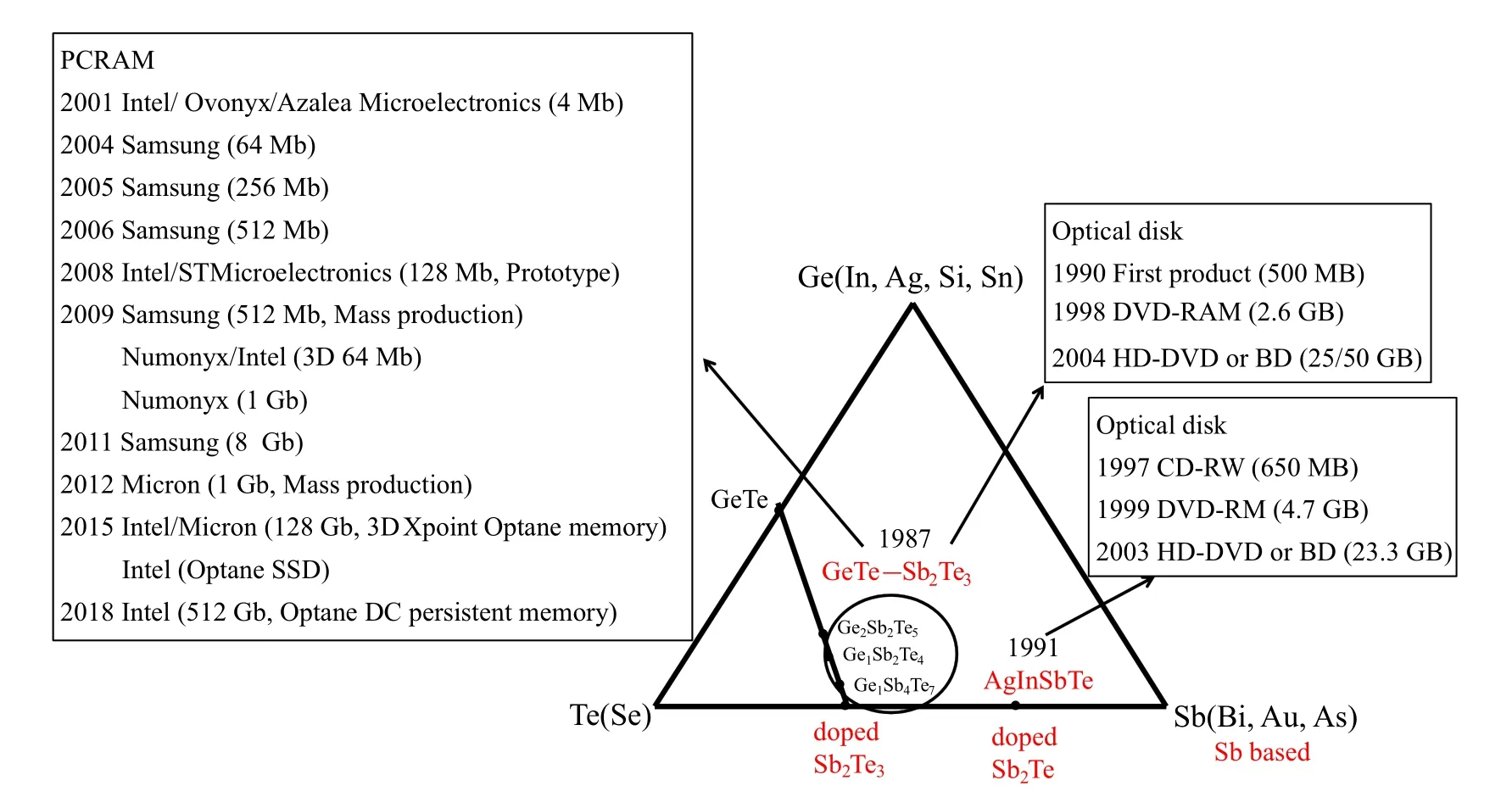
Fig. 5. Schematic ternary phase diagram depicting different phase-change alloys with their year of discovery and a summary of the development of optical and resistive phase-change memories. Reproduced with permission.[98] Copyright 2018,IOP Publishing.

Fig.6. Phase-change materials with different dopants into(a)GeSbTe-and(b)SbTe-based chalcogenides.
Doping a small amount of nitrogen into phase-change materials remarkably improves the write/erase cycling numbers of phase-change optical disk. The reason may be that nitrides are formed and condensed near the grain boundaries of Ge–Sb–Te microcrystals,which results in the formation of very thin wrappings to suppress the micro-material flow.[107]The nitrides formation has been confirmed by XPS,[135,136]high-resolution x-ray photoelectron spectroscopy and Ge Kedge x-ray absorption spectroscopy measurements.[137]Some experimental results show that interstitial N2molecules exist in the film, which plays a role in suppressing the crystalline grain growth.[138]The roles of doped nitrogen in GST film are to distort the crystal lattice, induce a strain field in the film, and refine the grain size through precipitation.[139]A two-step process including spherical-nucleation and diskshaped grain growth was found during the crystallization of GST film. However, nitrogen-doping into GST film suppresses the second step and the crystallization of GST-N contains only the primary nucleation process.[140]The phase transition from face-centre-cubic (FCC) to hexagonal (HEX)structure was delayed or even suppressed by nitrogen doping and the FCC structure unit cell is distorted due to nitrogen atom occupying the tetrahedral interstitial site because the volume of the tetrahedral site is not large enough for a nitrogen atom to occupy.[136]Nitrogen doping can increase the resistance of GST to some extent due to the grain refinement,[141]which results in the obvious scattering of current carrier by grain boundary. Two obvious steps were also observed in the resistance–temperature curve of GST-N film, which is very important for multilevel storage.[142]PCRAM chips based on GST-N show that low writing current and clear separation between SET and RESET resistance distributions was achieved[143]and the convergence of device resistance distributions was increased greatly.[144]
Carbon atoms are found to significantly enhance the thermal stability of amorphous GST by increasing the degree of disorder of the amorphous phase based on simulations[145]and experiments[146,147]because the carbon dopant forms a germanium carbide phase and atomic scale carbon clusters.[120]The FCC phase stability of the GST-C film was maintained by carbon doping after annealing at 440°C and the grain size of the GST-C film was significantly decreased due to the presence of carbon in the form of clusters or precipitating at the grain boundaries.[148]The microscopic C-doping role was unraveled based on ab initio calculations.[149]Carbon prefers occupying the interstitials at very low C concentrations and C atoms will cluster at the grain boundaries with very few C atoms existing at the interstitials when the C concentration is over 2%. With further increasing the C concentrations, C atoms tend to form ring-like configurations in the grain boundaries rather than chain-like configurations. The atom probe tomography(APT)technique was used to investigate the carbon distribution in GST-C.[150]APT results reveal the formation of plenty of GeC-based molecular clusters in the as-deposited GST-C,which leads to the remarkably improved thermal stability of GST-C. Moreover, these C-based bonds will break in the recrystallization process and form nanometerscale carbon clusters in crystalline GST-C. With the aid of advanced spherical aberration corrected transmission electron microscopy, the mechanism of microstructure evolution manipulated by C-dopant is clearly defined.[151]The grain-inner C atoms distinctly increase cationic migration energy barriers,which is the fundamental reason for promoting the thermal stability of metastable FCC phase and postponing its transition to the HEX structure. By current pulses stimulation,the stochastic grain-outer C clusters tend to aggregate in the active area by breaking C–Ge bonding;thus,grain growth and elemental segregation are effectively suppressed to improve device reliability resulting in >108cycles for 40-nm node 128-Mb chips based on GST-C.[150]
A third material family with very fast phase transition rate has been found that uses Sb based phase-change materials,such as GeSb,[152]SiSb,[153]ZnSb,[154]SnSb,[155]CSb,[156]or GaSb,[157]etc. However, the amounts of dopants should be controlled precisely. According to the latest report,[158]the amorphous problem of single element Sb as phase-change storage material has been solved by special technology and it can become a valid alternative when confined in extremely small volumes. This compositional simplification eliminates problems related to unwanted deviations from the optimized stoichiometry in the switching volume,which become increasingly pressing when devices are aggressively miniaturized.
Next, we will focus on the fourth material family that uses doped-Sb2Te3(ST) phase-change materials. Due to its high crystallization speed and low crystallization temperature,ST based chalcogenide semiconductors have already been widely used in rewritable optical disk.[159–163]The switching characteristics of doped SbTe[163]and ST[164]films for PCRAM application were first described in 2005. Various compositions of SbxTe phase-change films have also been investigated.[165]However, the stability of amorphous SbTebased phase-change materials is very poor and the applicability of a doped-SbTe composition for the phase-change line memory was first reported by Lankhorst, et al.[163]Although doping can reduce the phase-transition speed,doped-SbTe film can also obtain high-speed phase-transition performance as long as the doping degree is reasonably controlled, even at the expense of some phase-transformation speed. Doping one or more elements to SbTe-based chalcogenide has been studied widely (as shown in Fig. 6(b)). In particular, the doping modification of ST has become an important research hotspot of PCRAM with high speed and low power consumption.Both crystallization temperature and resistivity of amorphous ST increase after doping, which are beneficial for improving room temperature stability of the amorphous state and reducing the SET/RESET current of PCRAM.In short,Ge,Al,and N dopants sacrifice the phase-transition rate of ST too much,and the increase is not great compared with GST. The disadvantages of ST/Ta2O5, ST/HfO2, ST/SiN, and ST/SiC composite phase-change materials are mainly due to the poor stability and micro shrinkage caused by the composite of ST with large grain size and dielectric materials. Ag, Si, and Ti dopants have phase separation or delamination during phase transition,which is not desirable. The phase-change memory cell based on Ti0.4Sb2Te3alloy,showing one order of magnitude faster SET operation speed(6 ns)and as low as one-fifth RESET operation power, compared with GST-based phasechange memory cell at the same size.[185]Ti-centered octahedra(TCOs)not only disperse inside of the HEX ST lattice,but also form nano-lamellae separated outside, respectively acting as lattice distortion centers and nano-thermal insulators to induce low-energy amorphization of the restricted ST crystal grains. It was also identify that in amorphous Ti0.4Sb2Te3,the Ti atoms prefer to maintain the octahedral configuration.Such robust TCOs or nano-lamellae thus may serve as intrinsic nucleation centers or templates for surrounding Sbcentered atomic motifs to swiftly align into long range order to achieve high-speed recrystallization.[203,204]The PCRAM chip with Ti0.4Sb2Te3phase-change material was developed based on 12 inch (1 inch=2.54 cm) and 40-nm process.[205]The SET/RESET operation current and speed are better than the chip performance based on GST under the same conditions. However, in the process of improving the chip yield based on Ti0.4Sb2Te3phase-change material, Ti doping easily leads to the delamination of phase-change material,which leads to the improvement of chip yield becoming very difficult.Cr doping is beneficial to improve the crystallization temperature (235°C) and data retention of ST material (120.8°C,ten-year) and inhibit the grain growth under the premise of maintaining high speed.[193]On the basis of ab initio calculations, Y dopant for ST overcomes the phase-separation problem and significantly increases the phase stability and resistivity of crystalline state.[197]The maintained crystal structure of ST and the grain refinement provide the competitive fast crystallization speed of 6 ns for Y-doped ST.[206]Up to now,Sc-doped ST has the fastest phase-transition speed of 500–700 picoseconds for PCRAM.[58,59]This ultrafast crystallization stems from two factors being at work simultaneously. First,Sc-stabilized precursors serve as heterogeneous sites to catalyze nucleation,reducing the stochasticity and thereby accelerating the nucleation rate.[58]Second, the Sc-doped ST exhibits an enlarged kinetic contrast between elevated and ambient temperatures.[59]
5. Structure of PCRAM cell
As described in Section 3,the device structure has a great impact on many performance of PCRAM, such as operating current, power consumption, retention, endurance, speed, integration, SET and RESET resistance distributions, etc. In particular, many device structures are designed to reduce operating current and improve device integration. The best way to reduce the operating current is to design and optimize the structure of phase-change reversible resistor, which needs to follow the following basic principles: simple, feasible, scalable,good compatibility with semiconductor process,etc.
PCRAM cell structures tend to fall into one of two general categories: that which is called TOP-DOWN route depending on the semiconductor technology node and that is called BOTTOM-UP route depending on the self-assembling of nano-device, which is not compatible with semiconductor process. The TOP-DOWN route is widely used to design the cell structure and includes contact area minimization mode and phase-transformation volume minimization mode. The former mainly controls the cross section area by the size of the electrical contacts to the phase-change material,which may be named as contact minimized. And the latter mainly minimizes the volume size of the phase-change material itself within the cell by filling or confining the phase-change material into a pore opened in a dielectric material. The results show that compared with the contact-minimized device structures, the typical volume-minimized device structures have more advantages in thermal efficiency and the RESET current can be reduced by a factor 2, which shows that it has better application potential in low power consumption.[207]Some published PCRAM resistor device structure diagrams are summarized in Fig.7.
The most common contact-minimized cell structure is the mushroom cell,[208]where a narrow cylindrical metal electrode contacts a thin phase-change material film. The BE described as the “heater”, typically made of the most common interconnect electrode materials(such as TiN or W)in CMOS process, is the smallest part in this cell. The most important requirements for this structure are to minimize the diameter of the heater and select heater materials with suitable resistance,stability and thermal conductivity.Another contact-minimized cell structure is the edge contact cell,[209]whose contact area is determined by a thin film thickness in one dimension and very low programming current is achieved. It is because of the lateral contact characteristics of this structure that the element size is not small and the integration is limited. A cell structure named asμ-trench contact is the third contact-minimized cell structure.[210]The new key concept introduced in this architecture, that keeps the operating current low and maintains a compact vertical integration,which is beneficial for improving the integration. The contact area between the heater and the phase-change material is defined by the intersection of a thin vertical heater and a trench that is called“μ-trench”,which can be defined by sub-litho techniques and the heater thickness by film deposition. Therefore, the cell performance can be optimized by tuning the resulting contact area conveniently and a continuous improvement of power consumption is expected with the improvement of process nodes.
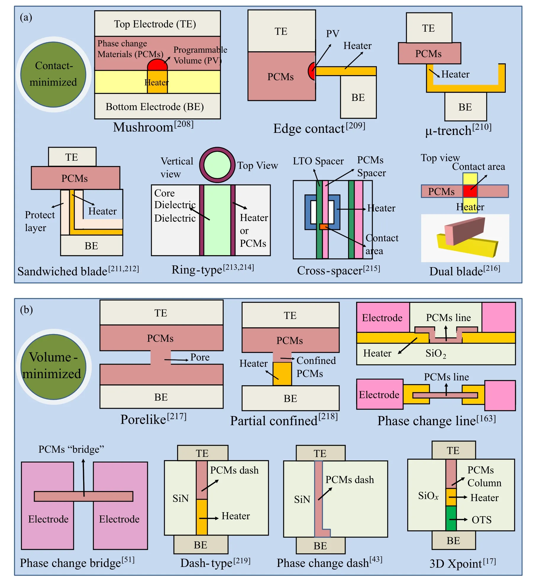
Fig.7. PCRAM device structures,(a)contact-minimized and(b)volume-minimized.
Moreover, optimizations of the heater material itself and thickness are proven to allow a reduction of the operating current, leaving room for further improvements. The μ-trench architecture has been integrated in a 90-nm 128-Mb array with programming currents of 0.3 mA of the storage element,which demonstrates the suitability of this structure for the production of high-density PCRAM arrays.[220]In order to prevent the heater in μ-trench structure from being oxidized by the surrounding oxide materials during the deposition process or SET/RESET operation,[221]resulting in the dispersion of heater’s resistance, a structure named as sandwiched blade heater was proposed.[211,212]The forth contact-minimized cell structure is the ring-type contact cell,which includes ring-type BE[213]and ring-type phase-change material.[214]The effective ring contact area is mainly related to the diameter and thickness of the ring,which makes the contact area of the ring less sensitive to the change of the ring diameter, because the relationship between the ring contact area and the ring diameter changes from quadratic to linear. Therefore, compared with the traditional cylindrical BE,the ring-type structure can improve the stability of the contact resistance. The ring-type BE technology was successfully used for high-density 256-Mb PCRAM.[222]It was clearly demonstrated that the ringtype BE results in very sharp distributions of SET and RESET resistances,a wide sensing margin,high manufacturability,and low RESET current. The fifth contact-minimized cell structure is the cross-spacer cell,whose contact area between phase-change material and heater is determined by the crossed area of both spacer sidewalls.[213,223]The ultra-small lithography independent contact area leads to low RESET current for competitive memory density and high performance. A similar but simpler dual blade structure is proposed.[216]The BE and phase-change material both with blade type are used to contact each other vertically to minimize the contact area, which is determined by BE and phase-change material film thickness.
In the early stage of PCRAM device fabrication,the typical volume-minimized cell structure was widely used. This structure is normally called as pore structure,[217]where a sublithographic hole formed in a dielectric material atop the BE is filled with the phase-change material.The electrically erasable nonvolatile memory with device area being limited to 10 μm openings in the polyimide film defined by photolithography was firstly reported.[224]In order to reduce the pore size and the operation current,focused ion beam(FIB)was used to fabricate the pore.[225,226]However, with the continuous reduction of pore size and the increase of aspect ratio, it is difficult to achieve good filling of phase-change materials in nano pores by using conventional physical vapor deposition processes. Therefore, it is necessary to develop new filling technologies for phase-change material, such as chemical vapor deposition or atomic layer deposition technology, to enable continued scaling of pore cell devices. In order to reduce the difficulty of nano-gap filling,the“partial confined structure”is another innovative idea for achieving low RESET current.[218]The main function of a partial confined structure is to reduce the difficulty of nano-gap filling for phase-change material and provide a better thermal environment for the PCRAM cell so as to lower the RESET current. The confined structure cell has a rectangular amorphous region after RESET operation according to the simulation results by two-dimensional finite element modeling.[227]The simulated results have also suggested that it is possible to drop RESET current further while increasing the depth of confined phase-change material and decreasing the corresponding contact size.[218]By using etching back process of heater,the partial confined structure was fabricated and is a promising candidate for high density PCRAM due to low writing current,good scalability,and insensitiveness to edge damage.[218,228,229]
A new volume-minimized memory concept, which is called the phase-change line memory, was proposed.[163]For the conventional PCRAM concept, the performance requirements for heating electrode are very high, such as easy to process, compatible with CMOS process, suitable resistance,high thermo-stability, no reaction with phase-change materials,and good adhesion with phase-change materials,etc. The requirements for electrodes in the line concept memory are relatively less and much less stringent because these electrodes are relatively large and will stay cooler. Also the processing technology of phase-change line memory is relatively simple, which requires only one or two additional lithographic steps on the basis of standard CMOS process. Similar to the line-concept memory cell, an ultra-thin phase-change bridge(PCB) volume-minimized memory cell, which consists of a narrow line of ultra-thin phase-change material defined by using electron-beam lithography(EBL)and ion-milling bridging two underlying electrodes,is demonstrated.[52]Different from the phase-change line memory,the two electrodes of the PCB memory are very close to each other,and the nano-gap in the middle is filled with dielectric materials. In this way,the very small cross-sectional area and volume of phase-change materials can be realized through ultra-thin and narrow sheet-shaped films, which is benefit for scaling down. However, for both phase-change line and bridge structures, the common disadvantage is that the integration is not high due to their horizontal structures. Therefore,a new vertical type volume-confined structure within 7.5-nm width dash-contact was proposed.[219]The RESET current was reduced below ~160 μA. In addition, the reliability and programming time was much improved due to the full volume confinement of PCRAM cell.Furthermore, a scalable volume-confined structure with only 10-nm width dash-type phase-change material was fabricated by using spacer and chemical mechanical polishing (CMP)technology with no fill-in issue.[43]In 2015, the proposal of 3D XPoint structure with the highest integration degree and suitable for 3D integration makes PCRAM structure reaches the most perfect level at present.[22]3D XPoint has crossbar structure with phase-change material, heater, and ovonic threshold switch (OTS) totally confined at the same size and yields a non-volatile memory with capacity available per CPU socket to as much as 3 TB,[26]which is a revolutionary technology for memory since 1989.
6. Large storage capacity
6.1. Scaling properties for phase-change material
The scaling limit of a PCRAM device mainly depends on the volume reduction limit of the phase-change material, and the phase transition can still reliably undergo with good stability and cycling endurance. Therefore,it is necessary to use a combination of theoretical simulation and experimental verification to evaluate whether the melting and recrystallization behavior of phase-change materials still meet the basic storage requirements of PCRAM when the volume of phase-change materials is reduced to nano scale and the interface effects start to prevail.[230]In order to explore the physical limit of the volume reduction of phase-change materials,many experimental methods have been used to prepare nano-scale phase-change memory cells, such as standard lithography technology,[231]EBL,[232]FIB lithography,[163,164,233]scanning probe microscopy (scanning tunneling microscope[234]and atomic force microscope[235]), BOTTOM-UP approach using phasechange material nanowires with small diameters,[236–244]ultra-thin PCB memory device concept,[52]and carbon nanotube electrode.[39,245]The carbon nanotubes are the best electrode materials to verify the volume limit of phase transition due to their small diameter, good conductivity, stability, and proper thermal conductivity,which can bring the lithographyindependent critical dimension down to 1.2 nm.[39]Good electrical characteristics obtained demonstrate the functionality and potential viability of PCRAM for highly scaled ultra-dense memory at least down to 2.5-nm node. In addition, two-dimensional materials, such as graphene,[246,247]sulfides,[248,249]and tellurides,[250,251]can also be used to integrate with phase-change materials in the form of edge contact and enable switching with low programming current due to the atomically thin films of layered materials. At the same time,the two-dimensional materials themselves may have switching characteristics and can be integrated with phase-change materials both as transistor and heating electrode,which will show high integration and ultra-low power consumption. However,the process will become more difficult and the stability of the device is not easy to control.
6.2. Multi-level-cell operation
Multi-level technology has been applied in NAND FLASH for a long time,which is a necessary scheme for new storage technology to obtain large capacity storage. Because the crystallinity of phase-change materials can change continuously, the reflectivity and resistivity also change continuously,which is very suitable for multi-level storage. The multilevel storage properties of phase-change materials have been successfully applied in phase-change optical disks realized by various methods,such as mark radial width modulation,[19,252]tangential mark-size modulation,[253]and run-length-limited modulation.[254,255]As early as 1997, Ovshinsky realized the 16 multi-level electrically induced reversible transformation of phase-change material in a single memory cell,which verified the feasibility of multiple-level-cell (MLC) application in PCRAM.[256]The microstructural changes induced by relaxation of phase-change material will lead to resistance drift,which is disadvantageous to MLC. Therefore, it is very important to control the resistance distribution and its drift of each state, which is the key for a successful MLC PCRAM.In order to control the resistance drift, it is necessary to unveil the structural origin of phase-change materials for resistance drift.[257]Several methods have been reported for obtaining different stable resistance states,such as doping modification of phase-change materials,[142]stacked multiple chalcogenide layers,[258–260]lateral phase-change memory,[261,262]parallel multi-confined cell structure,[263]waveform manipulation of programming pulse,[264,265]and program-and-verify(P&V)technique.[266,267]
It was shown that up to 16 intermediate resistance levels in a cell, i.e., 4 bit/cell can be programmed by varying the amplitude or slope of the trailing edge of the operating pulses,[264]whose feasibility are further verified by partial-SET programming[265,268]and partial-RESET programming.[269]Here, the partial-RESET programming is defined as that larger volumes of the amorphous region will be obtained by applying programming pulses of larger amplitudes,and the partial-SET programming is also defined in the same way as that the size of the amorphous volume will be shrinked by applying pulses of lower amplitude,or sequences of annealing pulses of appropriate magnitude to crystallize.Although the experimental results have revealed the reproducibility of the partial-RESET programming curve of a single cell,considerable spreads over a memory array have been observed.[269]Nevertheless,a P&V technique can be adopted to compensate for these spreads and improve the accuracy of programmed resistance levels.[266,267]In fact,the MLC design is a complex process, which can be described as a trade-off among several factors, such as resistance distribution, drift,temperature change,and sensing margin.[266]
6.3. 3D integration
The 3D storage based on phase-change materials was first applied in optical disk.[270]Multiple-layer phase-change optical disks have been realized with the aim of increasing their recording capacity.[271–274]For semiconductor memory,Moore’s law will soon fail as the size of process nodes gradually reaches the limit. The 3D technology is one of the mainstream technologies beyond Moore’s law to further increase the storage capacity. As one of the most important semiconductor memory,FLASH memory has developed rapidly in the past two decades,but it is also facing the challenge of further shrinking.[275]However, due to the limitation of its storage mechanism resulting in short-channel-effects and decreased number of stored electrons, it is difficult for planar NAND FLASH memory to further scale below the 10-nm process node. Therefore,the 3D NAND FLASH will be a solution in order to increase the memory density.[276]A 128-layer stack of 3D NAND FLASH memory was first announced by SK Hynix in 2019. The 3D PCRAM technology is also one of the best schemes for mass storage and the requirements for selectors are more critical because the reversible resistor of PCRAM cell can scale to 2.5-nm node at least. The performance of the three-dimensional integrated selector should meet the following conditions: a 4F2footprint, large On/Off current ratio (>104) with low leakage current and sufficient programming current density (>10 MA/cm2), good cycling, switching within the time comparable to the phase-change speed of PCRAM cell,compatible with CMOS process,etc.
So far, several selector candidates have been proposed and the most promising ones are a Si-based diode[277–281]and an OTS.[282]In particular, OTS has the most practical value and has become the research hotspot of 3D PCRAM selector. Ovshinsky discovered the switching and memory effect of the amorphous materials in 1968.[17]It involves OTS[283]and ovonic memory switching (OMS).[284]The typical current–voltage(I–V)characteristics of PCRAM are shown in Fig.8,which contains OTS and OMS.[32,99]OTS is related to the reversible switching mechanism between an electrical low conductive state with very small leakage current and a high conductive one with sufficient current. The structure of the material is always kept in amorphous state during the switching process even though the applied voltage reaching the threshold value Vth. The resistance returns to the high value again when the applied voltage is released. Different from OTS,OMS refers to the reversible transition between the stable high resistance amorphous state and the low resistance crystalline state. After the applied voltage is removed, the material cannot return to the amorphous state automatically because the structure of the material has changed into a stable one,but always remains in the crystalline state unless additional RESET pulse is applied to induce the phase change. PCRAM is just based on this OMS effect of phase-change material to store binary information in a nonvolatile memory device.

Fig. 8. Schematic I–V characteristics of a threshold switching device and a PCRAM.In the case of threshold switching(OTS)indicated by the green arrows, the device switches back to the high-resistance state at a low voltage. In the case of memory switching (OMS) indicated by the red arrows,the low-resistance state is retained even at 0 V.The operation process of SET and RESET is completed along the direction indicated by the red and blue arrows respectively.
The emerging OTS materials and their performance in devices, especially potential switching mechanism have been reviewed and discussed in detail.[285]It is generally believed that the threshold switching mechanism of OTS is a purely electronic process,which is consistent with Ielmini’s theoretical model.[286]However,there are still many doubts about the threshold switching mechanism of OTS, which is helpful to the development of new materials for OTS and the optimization of device performance.
The first 3D PCRAM chip consisting of a storage element (PCRAM cell) and a selector (OTS) was introduced in 2009,[282]and the physical construction of a memory cell is shown in Fig.9.[287]
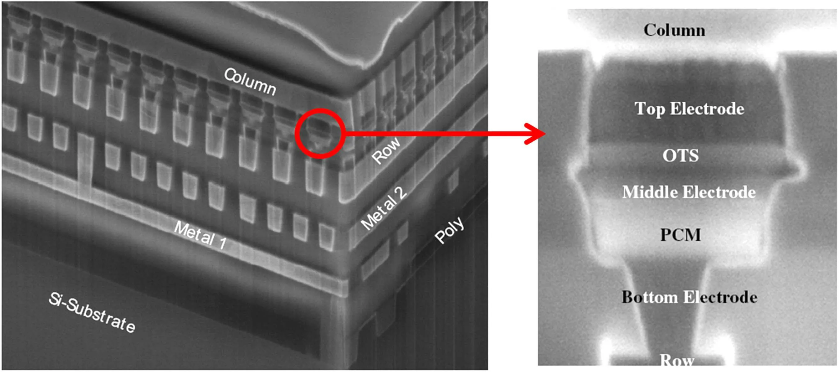
Fig.9. One layer of the PCRAMS array fully integrated with a CMOS technology and SEM cross-section of a PCRAM cell between rows and columns.Reproduced with permission.[287] Copyright 2019,IOP Publishing.
Based on this structure,the two-layered 3D XPoint memory (Fig. 10(a)) named as Optane memory with capacity of 128 Gb per die was announced by Intel and Micron.[22]Furthermore, Intel announced a new class of Optane memory named as Optane DC Persistent Memory with packages of up to 512 Gb per stick in 2018.[26]Intel has built a platform with 192-GB memory, 1-TB Optane DC memory (Fig. 10(b)) and attached to SATA/NVMe SSD for remote access. The biggest features for 3D XPoint memory are 1000×more durable than NAND FLASH while simultaneously offering a 1000× performance increase and hitting densities at least 10× greater than DRAM,which means that 3D XPoint memory has the capability of bridging the gap between DRAM and non-volatile storage in the future(Fig.10(c)). The OTS used in 3D XPoint memory was Se–Ge–Si-based alloys doped with As,[24]which have good thermal stability,low leakage current and good endurances. However, these OTS devices rely heavily on intricate control of material stoichiometry and generally suffer from toxic and complex dopants. A new binary OTS selector device based on C–Te exhibits outstanding performance such as a high switching ratio, an extremely low off-current,an extremely fast operating speed, high endurance, and high thermal stability.[288]By introducing a thin amorphous Ge layer between the top/bottom electrodes and the C–Te-based binary OTS film, considerable device performance improvements such as a nearly 2-order of off-current reduction and tight distribution of Vthand off-current, resulting in uniform switching characteristics, were achieved.[289]Recently, a selector based on GeS, an environment-friendly binary semiconductor, was reported and has large drive current density(34 MA/cm2)due to the strong Ge–S covalency and high nonlinearity(~106)arising from the synergy of the mid-gap traps assisted electronic transition and local Ge–Ge chain growth as well as locally enhanced bond alignment under high electric field.[290]

Fig.10. (a)TEM cross-section of two-layered 3D XPoint memory. (b)Photo of 3D XPoint memory released by Intel in 2018. (c)Optane DC memory will bridge the gap between DRAM and non-volatile storage.
7. Optoelectronic hybrid storage
According to the latest development of PCRAM,phase-change materials can achieve switching time of subnanosecond and can be scaled down further to a few nanometers, which may make PCRAM to lead to electronic devices with improved computing efficiency by simplifying the memory hierarchy without massive data transfer between nonvolatile memories and DRAM/SRAM.In order to achieve this goal, improvements on performance of PCRAM in terms of access time and storage density are still being pursued although great progress has been made in the above-mentioned phase-change materials and storage capacity.
7.1. Concept for optoelectronic hybrid storage
From the basic operation principle of PCRAM,it can be seen that the SET process of PCRAM involves the crystallization of phase-change materials,which is the bottleneck of PCRAM operation speed. At present,the experimental methods used to induce the crystallization of phase-change materials mainly include thermal annealing, laser induction and electric pulse induction. Thermal annealing is only used to study the basic crystallization properties of phase-change materials. The crystallization is sufficient, but it takes a long time (more than seconds). In phase-change rewritable optical disk, the pulse width of a laser beam being used to induce phase change can be short as picosecond and femtosecond, and the reversible phase change can be also realized using such short laser pulse,[291]which means the write/erase time can be scaled down to picosecond and even femtosecond. However, the reflectivity contrast between amorphous and polycrystalline state is not large enough and the carrier to noise ratio of information storage is very limited. While for PCRAM, the electrical resistance contrast between amorphous and polycrystalline state is very large with about one order of magnitude,which can obtain high carrier to noise ratio of information storage and be beneficial for MLC. However, the shortest pulses reported for electrical excitation of a PCRAM device based on GST are only of 500 ps duration[57]although the threshold switching can take place within the electric pulse on sub-picosecond time scales by using few picosecond single-cycle electromagnetic waves to optically apply an electric field to the PCRAM.[292]Due to its thermal effect phase-transition mechanism, PCRAM cannot meet the requirements of ultra-high speed storage. So the question comes out that if we can combine the advantages of phasechange rewritable optical disk and PCRAM into one memory? In other words, if the reversible phase change induced by laser is used to write and erase the information, and the change of resistivity of phase-change material can be used to realize the accurate reading of information. This is the so-called optoelectronic hybrid storage phase-change memory with optical writing and electrical readout, which can give full play to the advantages of traditional optical storage and electrical storage, and realize the purpose of ultra-high speed storage.[293]The display and data visualization applications that go beyond data storage were firstly created by combining the optical and electronic property modulation of phase-change materials.[294]However, integrating both electrical and optical modulation functionalities effectively into a single memory device based on current semiconductor process capability has so far proved elusive because the requirements of size-limited electrical switching and diffraction-limited optical response are in conflict.[295]According to the requirements of optoelectronic hybrid storage, the following problems need to be solved: i) new phase-change materials with high phase-change speed,high data retention and high resistivity contrast;ii)ultrafast phase-transition mechanism of phasechange materials in picosecond/femtosecond time scale; and iii)realization of optoelectronic hybrid memory device.
7.2. Phase transition induced by femtosecond laser
The phase transition of phase-change materials induced by ps/fs laser has been widely studied. The phase change induced by a picosecond or nanosecond laser pulse is a classical thermal process containing three distinct stages, namely,rapid melting, solidification, and slow relaxation.[296,297]So there is no more discussion about this here. The interaction between femtosecond laser and phase-change material is very difficult to capture due to the ultra-short pulse width of femtosecond laser. However, non-thermal melting and a loss of long-range order up to 90 nm inside the InSb semiconductor was measured successfully at femtosecond resolution,which enables the possibility in the study of ultrafast dynamics in phase-change material.[298]The total time of applying energy is much shorter than the heat diffusion time and phase-change time when femtosecond laser irradiates on a sample. Therefore, crystallization and mark formation are mainly determined by the instantaneous deposition of laser energy,which provides the ability to tailor the number of pulses in addition to the laser fluence to control the crystallization process[299]and to realize multi-level crystallization.[300,301]For partially amorphized GST films, recrystallization can be induced by a single pulse with width of 100 fs because the existing crystalline grains play a key role in accelerating crystallization.[302]In addition, compared with the conventional laser pulse, femtosecond laser pulse has much higher peak energy,which can create small highly excited plasma before energy transfers from the excited carriers to the lattice.Therefore,the electronic excitation can be significant and the structural transition under femtosecond laser pulse can be initially non-thermal in nature.[302]By employing a femtosecond laser double pulse with an adjustable inter-pulse delay,the lifetime of excited electrons in melt-quenched amorphous GST can be estimated to be about 100 ps.[301]Note, however,that even when ultrafast non-thermal melting occurs,the electrons and the lattice reach thermal equilibrium typically within a few picoseconds so that subsequent resolidification of the material on a much longer time scale is still a thermal process.[303,304]This statement is further confirmed by the carrier dynamics of amorphous GST films, whose carrier relaxation consists of two components:a fast process dominated by an intraband carrier relaxation and the carrier trapping within 5 ps and a slow recombination process of trapped carriers after 5 ps.[291]The crystallization behavior of amorphous GST induced by nanosecond laser and femtosecond laser is quite different.[305]For single laser pulse irradiation, it is columnar growth behavior and neither tetrahedral nor off-octahedral positions of Ge-atoms were detected in the defect-free grains,while the crystallization after nanosecond laser single pulse irradiation shows oval grains formation. Recently, the phasetransition process in picosecond time scale has been observed by ultrafast transmission electron microscopy in real time,[306]which is very useful for studying the ultrafast phase transition of phase-change materials.
Femtosecond laser can also induce the amorphization of phase-change materials, and has obvious advantages, such as a complete amorphization with sharp borders between amorphous and crystal phases and a more efficient energy deposition.[307]Due to the higher supercooling, a complete amorphization can be achieved by using a single femtosecond laser pulse with width of 85 fs for GST films[299]and 130 fs for Cr-doped ST films.[194]Amorphization can also be realized without passing through the molten phase, in form of a photo-assisted process generating sufficiently high carrier densities to trigger the phase transition[308–310]or a collapse of long-range order triggered by distortions in the crystalline phase.[311]
7.3. Phase-change materials for optoelectronic hybrid storage
Although GST is the most mainstream phase-change material,it has many advantages,such as stable composition and high cycle times,and has been successfully applied to phasechange optical disk and PCRAM. However, due to its disadvantages in phase-change speed, data retention, and power consumption, GST is not the optimal phase-change material for optoelectronic hybrid storage. Interfacial phase-change memory (iPCM) consists of a superlattice (SL) structure(Figs. 11(a) and 11(b)[312]) formed from alternating layers of GeTe and ST.[313]iPCM was designed to utilize a solidsolid phase transformation between the covalently bonded(amorphous) and resonantly bonded (crystalline) phases, induced predominantly by the displacement of Ge atoms at the interface, to achieve both faster and lower power threshold switching than in conventional GST alloys.[310]In the early stages of the non-thermal pre-amorphization under repetitive photo-excitation, the bonding coordination around Ge atoms in the iPCM system becomes unstable due to the coherent modulation, resulting in two different coordination environments, which relax within a few picoseconds and show the ability of ultrafast switching.[314]The phase-change material with SL structure with significant advantages of low power consumption,[315]high speed, and good cycling performance(Fig.11(c)[316])may be an optional material for optoelectronic hybrid storage because the structure of SL can be kept well due to the non-melting phase transformation from crystalline to amorphous phase.[310]GeTe/ST superlattices have been investagated intensively till now.[317–324]Other SLL structure phase-change materials, such as Bi2Te3/ST,[325]Ge/ST,[326]GeTe/Sb7Te3,[327]Si/Sb80Te20,[328]GeTe/GST,[329]GST/SiO2,[330]Ga30Sb70/Sb80Te20,[331]GeTe/InTe,[332]SnxTe100?x/ST,[333]Si/Sb,[334]Ge40Te60/Cr,[335]and Ge8Sb92/Ge[336]were also reported having much better switching speed and thermal stability in comparison with GST.Cr-doped ST film may be one of the best phase-change materials candidates for optoelectronic hybrid storage due to its high crystallization temperature(235°C),good data retention(120.8°C, ten-years), and lower power consumption.[193]In addition, amorphization by a single femtosecond laser pulse with 130 fs and crystallization by multiple femtosecond laser pulse with time of about 5 ps can be realized for Cr-doped ST films, which shows the potential of high-speed application in optoelectronic hybrid storage.[194]
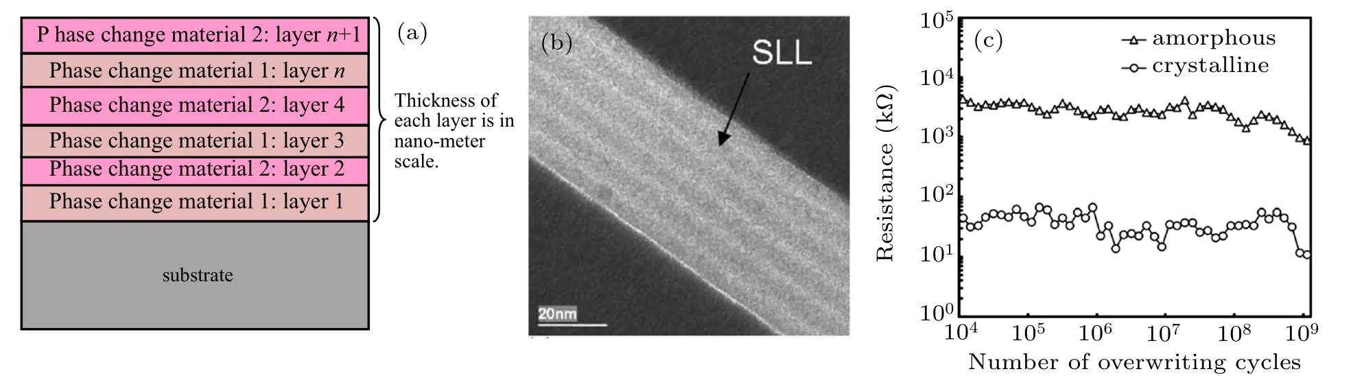
Fig.11. (a)The diagrammatic sketch of SL structure. (b)Transmission electron microscopy photo of SL structure. Reproduced with permission.[312]Copyright 2006, AIP Publishing LLC. (c) Cycle endurance of an SL cell. Stable and reversible switching of the cell is observed for 109 overwriting cycles. Reproduced with permission.[316] Copyright 2010,AIP Publishing LLC.
7.4. Prototype device for optoelectronic hybrid storage
In order to realize phase-change optoelectronic hybrid storage, it is necessary to integrate ultra-short pulse laser with phase-change storage cell effectively,especially based on silicon-based integrated technology, so as to reduce the manufacturing cost and improve the practicability. In the past few years, non-volatile photonic devices based on phase-change material have been widely studied and their research progresses have also been reviewed comprehensively.[104,105]A great deal of efforts has been devoted to exploring on-chip storage photonic devices using phase-change materials. The first generation of on-chip photonic devices saw the beginning of phase-change photonic resonators,whose particular design involves over-cladding GST media on a silicon(Si)racetrack resonator, as illustrated in Fig. 12(a).[337]These innovative ideas inspired the development of a true all-photonic nonvolatile memory comprising a thin GST film coated by an indium tin oxide(ITO)film to protect the GST layer from oxidation as shown in Fig.12(b).[338]Compared with its electronic counterparts, the phase-change photonic memory has several advantages,such as ultra-fast all-optical storage with an ultralow power consumption,[339,340]good down-scalability, and high density multi-level storage,[341,342]which enable its application in on-chip computation and phase-change photonic neuro-networks. However,the write–erase times are between 0.7 ns and 20 ns and also the information reading relies on the large difference between the refractive index of amorphous and crystalline states,which means that the read process is still optical readout. The complex link between the electronic and optical properties in a novel proof-of-concept device was provided for the first time, leading the way for the development of further applications based on mixed-mode electro-optical operation.[343]Here,the optoelectronic device can be operated in electro-optical mixed-mode by electrically induced crystallization and reamorphizing the phase-change material optically while the two different repeatable states are shown by the resistance values. By combining plasmonics, photonics,and electronics,a mixed-mode plasmonic phase-change memory cell integrated in a photonic waveguide as shown in Fig.13 was proposed and can be electrically or optically switched between binary or multilevel states.[295]Crucially, this device can also be simultaneously read out both optically and electrically, which makes it much closer to the prototype concept device of phase-change optoelectronic hybrid storage.
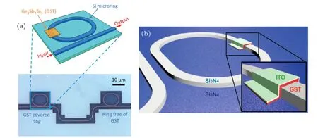
Fig.12. (a)Optical microscope image showing the two microrings coupled to a waveguide. The first of them(top)contains the overladding layer of GST.Reproduced with permission.[337] Copyright 2013,AIP Publishing LLC.(b)3D scheme of a hybrid nanophotonic phase-change material circuits using partially etched ridge waveguides in Si. Reproduced with permission.[338] Copyright 2014,WILEY-VCH Verlag GmbH&Co.

Fig.13. (a)3D illustration of mixed-mode plasmonic memory cell integrated in a photonic waveguide. Light is delivered to the nanoscale device via a photonic waveguide,while the Au contacts serve as both device electrodes and plasmonic nanogap to focus incoming light. (b)Illustration of device programmed using an optical signal with both electrical and optical readouts of the device state. (c)Real-time trace of the device’s optical transmission during multiple write and erase cycles. (d)Simultaneous readout of the device’s electrical resistance showing nonvolatile switching of the GST between the amorphous and crystalline states. Reproduced with permission.[295] Copyright 2019,AAAS.
8. Conclusion and perspectives
Over the past two decades, PCRAM has evolved from a prototype device to the most mature new nonvolatile memory capable of increasing the computing efficiency of electronic devices. The goal is to revolutionize von Neumann computing architecture and to develop universal memory to cope with the data explosion crisis.To achieve this goal,on the one hand,the performance of PCRAM,such as speed,capacity,power consumption,and cost,should be improved greatly. On the other hand, optoelectronic hybrid storage based on phase-change material may be an effective solution. However, some problems need to be solved: (i) new phase-change materials with high phase-change speed,high data retention and high resistivity contrast;(ii)ultrafast phase-change mechanism under nonequilibrium dynamics condition in picosecond/femtosecond time scale;and(iii)prototype devices and products realization of optoelectronic hybrid memory.
In the future, optoelectronic hybrid storage based on phase-change material may be realized by using silicon-based photonics technology because of the merits faster operation speed, larger capacity, more stable properties, and lower energy consumption. Once the device technology has made a breakthrough, the optoelectronic hybrid memory will completely replace DRAM, SRAM, and FLASH as a universal memory and will be applied in the field of merging computing(in-memory computing[344,345]and neuro-inspired computing[346–348]) and communications technologies due to its high-speed, low-power consumption, high-capacity, and non-volatile.
Acknowledgment
Prof.Liu B acknowledges Prof.Wuttig M for his valuable advices.
猜你喜歡
毛紡科技(2023年1期)2023-02-24
Chinese Physics B(2022年11期)2022-11-21
做人與處世(2022年2期)2022-05-26
兵器知識(2019年1期)2019-01-23
赤水源(2018年6期)2018-12-06
航空世界(2018年12期)2018-07-16
商周刊(2017年16期)2017-10-10
軍工文化(2017年12期)2017-07-17
今古傳奇·故事版(2016年22期)2016-12-24
- Chinese Physics B的其它文章
- Corrosion behavior of high-level waste container materials Ti and Ti–Pd alloy under long-term gamma irradiation in Beishan groundwater*
- Degradation of β-Ga2O3 Schottky barrier diode under swift heavy ion irradiation*
- Influence of temperature and alloying elements on the threshold displacement energies in concentrated Ni–Fe–Cr alloys*
- Cathodic shift of onset potential on TiO2 nanorod arrays with significantly enhanced visible light photoactivity via nitrogen/cobalt co-implantation*
- Review on ionization and quenching mechanisms of Trichel pulse*
- Thermally induced band hybridization in bilayer-bilayer MoS2/WS2 heterostructure?