
The 3D nanoimaging beamline at SSRF
2024-01-10 10:53LingZhangFenTaoJunWangRuoYangGaoBoSuGuoHaoDuAiGuoLiTiQiaoXiaoBiaoDeng
Nuclear Science and Techniques 2023年12期
Ling Zhang · Fen Tao · Jun Wang · Ruo-Yang Gao · Bo Su · Guo-Hao Du · Ai-Guo Li · Ti-Qiao Xiao · Biao Deng
Abstract Full-field transmission X-ray microscopy (TXM) is a powerful non-destructive three-dimensional (3D) imaging method with a nanoscale spatial resolution that has been used in most synchrotron facilities worldwide.An in-house-designed TXM system was constructed at the BL18B 3D nanoimaging beamline at the Shanghai Synchrotron Radiation Facility.The beamline operates from 5 to 14 keV and enables 20 nm spatial resolution imaging.The characterization details of the beamline are described in this paper.The performances in terms of spatial resolution, nano-CT, and nano-spectral imaging of the TXM beamline are also presented in this article.
Keywords Transmission X-ray microscopy (TXM) · Nano-CT · Synchrotron radiation
1 Introduction
Full-field transmission X-ray microscopy (TXM) is one of the most powerful tools for observing the internal structures of objects at the nanometer scale.Utilizing the high throughput and energy tunability of synchrotron X-rays, TXM offers a number of unique advantages, such as high penetration and spatial resolution, making it superior to other imaging techniques (scanning electron microscopy, atomic force microscopy, etc.) in testing thick samples [1–3].
Aimed at providing advanced nanostructure characterization and research methods for users in the fields of materials,energy, environment, etc., the Shanghai Synchrotron Radiation Facility (SSRF) planned to design and manufacture a TXM device.Table 1 shows the design objectives of this beamline.In December 2021, the X-ray 3D nanoimaging beamline (BL18B) was completed.Based on TXM, this beamline can provide complementary and unique capabilities to current microscopy research methods for studying crucial scientific problems, such as the structural and property changes of lithium battery materials in the charge–discharge cycle, relationship between micro- and nanoscale pores, and reservoirs of shale gas [4–14].This beamline covers an energy range of 5–14 keV and achieves a spatial resolution of 20 nm.The main research methods for this beamline include TXM, nano-CT, and nano-spectral imaging.The characterization and experimental methods are presented herein, including some initial operational results.
2 The beamline
The overall design of the beamline is formulated according to the scientific goals of the beamline and user requirements.Key considerations include the photon flux, energy resolution, and matching of the phase space.
The photon flux is a key factor in determining the data quality and time resolution of imaging experiments.Therefore, maximizing the photon flux at the sample while ensuring energy resolution and phase-space matching is the basic principle of beamline design.Considering the insertion device resources in the SSRF and phase space for the TXM,a bending magnet was selected for this beamline.In cases where light sources, monochromator crystals, and condensers have been selected, the main consideration is thetransmission efficiency of the beamline optics.The main factors affecting the photon flux include the receiving angle of the beamline, coating reflecting surfaces of the mirrors,angle of incidence of the beam on the mirrors, and the reception efficiency of the condenser.

Table 1 The design goals of BL18B
Zone plate (ZP) imaging systems require monochromatic incident light sources to satisfy Δλ/λ≤ 1/N[15], where Δλis the illumination radiation spectral width,λis the incident X-ray wavelength, andNis the zone number.Spectral imaging technology combining TXM and XANES requires an energy resolution higher than 2 × 10⁻⁴.The main factors that affect the energy resolution include the Darwin width of the double-crystal monochromator (DCM) crystal, vertical divergence angle of the incident beam on the first crystal of the DCM, and heating deformation of the first DCM crystal.Additionally, the slope errors for the mirrors and DCM must be minimized.
According to the characteristics of beam propagation in the ZP imaging microscope, the overall optical path was divided into two segments.The first segment is the beamline system from the light source to the secondary light source.In this section, the horizontal and vertical phase spaces propagate independently and approximate the conservation.The second segment is the ZP imaging system from a secondary light source to the detector.This segment is an axisymmetric optical system, and the phase space is approximately conserved within a radius perpendicular to the optical axis.An important task in optical design is to assemble the beam into the desired shape according to the principle of conservation of the phase space and deliver it to the sample.
2.1 Light source
BL18B is a bending magnet (BM) beamline with 1.27-T magnetic field strength.To ensure that the X-ray beam reaching the TXM end station is of the desired width and angle in both the horizontal and vertical planes, the angular acceptance of this beamline is set to 0.4 mrad × 0.22 mrad.The specifications of the BL18B light source are listed in Table 2.Figure 1 shows the brilliance and flux curves of the SSRF BM sources.The estimated source brilliance is 6.48 × 10¹⁵phs/s/0.1%bw/mm2/mrad2at 8 keV, with a total flux of 1.19 × 10¹³phs/s/0.1%bw.

Table 2 Specifications of BL18B Light source
2.2 Beamline optical design
Figure 2 shows the overall layout of the beamline.There are two major hutches: an optical hutch and an experimental hutch.As shown in the figure, the beamline houses a collimating mirror (CM), DCM, and toroidal mirror (TM) for pre-focusing.The CM was located 20.2 m downstream of the source.After the CM, the Si(111) DCM was placed at 23 m downstream of the source.After the DCM, the vertically collimated beam passed through the TM, which was located 26 m from the source, and was then focused onto a slit located 39 m from the source.This slit was located at the experimental station and was the secondary source aperture (SSA).
2.2.1 Mirrors

Fig.1 Brilliance and flux vs.photon energy of the bending magnet with acceptance angle 0.4 mrad(H) × 0.22 mrad(V)

Fig.2 (Color online) Schematic of the beamline layout
The vertical CM is the first optical component of the beamline.It receives white-beam radiation from the source and provides parallel illumination in the vertical plane for DCM.It has three functions: to reduce the power of the incident beam to the DCM, reject higher-order harmonics from the BM spectrum, and collimate the incident X-rays well below the Darwin width of the Si(111) DCM.CM was realized by bending a plane mirror, and the incident beam is collimated and reflected upward.To ensure an adequate level of power reduction to the DCM and effective harmonic rejection required for the X-ray microscopy experiments, an Rh coating was used for the CM reflective surface.Water cooling is sufficient to solve the power reduction problem.The CM operates at a fixed 4.4 mrad incidence angle, leading to a cut-offenergy of approximately 15 keV.According to the vertical receiving angle of the light source (0.22 mrad)and 4.4 mrad grazing incidence angle, the optically active length of the CM was 1000 mm.To minimize the diffusion of the focusing beam at SSA and maintain the reflectivity of the mirror at higher than 95%, the surface roughness of CM should be higher than 3 ?.The root mean square (RMS)slope error of the CM is required to be less than 0.8 μrad along the meridional direction (including the mechanical error 0.6 μrad and gravity and deformation error 0.2 μrad),and the RMS slope error along the arc direction is required to be less than 5 μrad.
The TM was realized by gently bending the cylindrical mirror to the required shape.It collected a monochromatic beam and delivered both horizontal and vertical foci to the SSA.The beams received by the TM are parallel in the vertical direction and divergent in the horizontal direction.Therefore, the incident beam is reflected downwards and is focused to 100 μm (H) × 290 μm (V) (full width at half maximum @8 keV) at the SSA position.As the TM was placed behind the DCM, it had no cooling requirements.The coating, grazing incidence angle, surface roughness, RMS slope error, and optically active length of the TM were identical to those of the CM.
2.2.2 Double-crystal monochromator
The DCM was placed horizontally between the two mirrors.The beam was collimated in the vertical plane before and after passing through the monochromator.Two major technical concerns for the DCM are: to achieve an angular stability of the diffracted beam of 0.5 μrad or higher and to minimize the thermally induced slope error on the first crystal.The DCM was equipped with standard Si(111) double-plane crystals to provide adjustable energy within the range of 4–15 keV and a high energy resolution higher than 2 × 10⁻⁴, which meets the requirements of the ZP objective in TXM.The DCM is a domestic monochromator adopting a common design used in the SSRF.The two crystals have an(n–n) achromatic arrangement.During the energy scan, the position and direction of the outgoing beam were maintained constant, and the height offset between the incident and outgoing beams was 25 mm.The main axis of Bragg rotation was located in the first crystal.As DCM performs Bragg rotation, the second crystal moves in the direction normal to the crystal surface [16].The thermal deformation of the first monochromator crystal reduced the flux, energy resolution, beam size at the SSA, and matching efficiency of the condenser in the TXM end station.The thermally induced RMS slope errors along the arc and meridional directions must be less than 5 μrad.According to the calculated results,the power absorbed on the first crystal can be comfortably managed by water cooling.
3 TXM end station
The experimental hutch houses the SSA, detector system for the beam intensity, and TXM system.The beam detector system comprised two ion chambers located downstream of the SSA to monitor the incident flux.Figure 3 shows a photograph of the TXM system comprising a monocapillary condenser, pinhole, objective ZP, sample station, and two X-ray imaging detectors.The condenser,located approximately 2 m from the SSA, was a singlebounce ellipsoidal glass monocapillary.The BL18B adopts an in-house-designed monocapillary as condenser [17, 18].The monocapillary condenser provided hollow-cone illumination to match the numerical aperture of the ZP, with a beam stop attached to its upstream end.For beamlines at third-generation synchrotron radiation sources, the beam emittance in the vertical plane is typically lower than the required microscope acceptance.This mismatch causes some sample areas to be illuminated or the beam angle to be insufficient to fill the objective lens.To overcome this problem, a shaker was installed under the condenser chamber to perform fast scanning and to expand the illumination angle of the sample to match the numerical aperture of the ZP.

Fig.3 (Color online) TXM system: a condenser, b pinhole, c sample holder, d ZP, e high-resolution detector, f medium-resolution detector.Other components are: g in-line telescope, h vacuum pipes
A pinhole upstream of the sample was employed to block the direct light that was not focused by the monocapillary condenser.It was positioned on a motorized stage between the condenser exit and sample.Pinholes with diameters of 100 and 150 μm were mounted on a single holder.
The sample stage comprises a high-precisionxyzmotor and an air-bearing rotation stage.The sample holder was placed on a breadboard mounted on a sample stage.
The microscope objective ZP produces a magnified image of the sample.The image resolution was determined using the outermost zone width of the ZP.For TXM imaging in BL18B, two sets of ZPs with an outermost zone width of 25/40 nm, diameter of 125/150 μm, and Ir thickness > 0.7/0.9 μm (XRnanotech, Switzerland) were used.
The BL18B has two sets of X-ray imaging detectors for high- and medium-resolution imaging.The high-resolution detector is a scintillator-coupled optical microscope with 2×, 4× and 10× optical magnification lenses and a watercooled 16-bit 2048 × 2048 camera (Zyla 4.2 PLUS sCMOS,Andor, Oxford Instruments, UK) with 6.5 μm square pixels.It was installed on a linear track with a travel range of 1.3 m along the beam direction, providing greater flexibility in the distance between the ZP and detector.The other detector with 2048 × 2048 pixels and 6.5 μm/pixel (12849-1111U, HAMAMATSU, Japan) was fixed at the back end of the hutch.The two detectors can be switched according to experimental requirements.
An in-line telescope was placed on the optical platform for sample positioning.Vacuum tubes were placed between the ZP and detector to minimize the attenuation of X-rays in the air.

Fig.4 (Color online) Schematic of a TXM
Each component of the TXM system was mounted on a highly stable marble optical platform with the relative position of each component fixed.To minimize the effects of acoustic vibrations, airflow, and temperature changes on the experiment, a Plexiglas enclosure was placed on the platform.The enclosure has sliding doors to facilitate operations such as changing the samples.
3.1 Imaging technologies
The primary imaging technologies of this beamline include TXM, nano-CT and nano-spectral imaging.Nano-CT is a non-destructive imaging protocol used to generate high-resolution 3D images comprising two-dimensional (2D) projections or "slices" of micrometer-scale samples.Nano-spectral imaging is a technique that combines TXM with X-ray absorption near-edge structure (TXM-XANES) to detect 2D and 3D chemical phase transformations in mesoscale volumes at the nanoscale [19, 20].It is worth mentioning that the combination of CT and spectral imaging can enable joint characterization of the morphology and chemical states of the sample, which makes it possible to better study the material properties.
3.1.1 TXM
Figure 4 shows the schematic of a TXM.A monocapillary condenser delivers a focused beam onto an object (sample).A pinhole cleans the beam and blocks the direct light not focused by the capillary.A ZP magnifies and images the sample onto a detector.TXM with nanoscale resolution can meet the micron-level field of view and nanoscale resolution.
Based on two detectors, the BL18B beamline TXM method has two resolution modes, high- and medium-resolution modes, which can realize sub-20 nm and sub-70 nm spatial resolution [21].
3.1.2 Nano-CT
Nano-CT is a useful method for studying the fine structure of materials.Unlike micron-scale resolution experiments,nanoscale resolved TXM samples are smaller and require finer preparation.Therefore, they should be prepared carefully.For ZP-based TXM CT imaging, the thickness of the sample should be less than the depth of focus (DOF), which is defined by DOF = ±λ/2 (NA)2 = ± 2Δr2/λ, whereλis the incident X-ray wavelength,NAis the ZP lens numerical aperture, and Δris the outermost zone width of the ZP [22].When a portion of the sample was outside the DOF, the ZP could not focus the out-of-range portion.
For the BL18B, suitably sized powder samples were gently blown onto stretched glass capillaries.The bulk sample was cut to the appropriate size and firmly fixed on the tip of a needle using a focused ion beam (FIB) or other fine sample preparation methods.Since the sample size was in the micron range, an offline light microscope was used to roughly examine the sample preparation.Figure 5 shows a photograph of the gold particles in the stretched glass capillary and their 2D projection.The capillary tube or needle was firmly clamped to the center of the sample holder, and remained stable during the CT experiments.
The CT results of BL18B were processed using a completely in-house designed automatic projection alignment algorithm [23] and in-house designed reconstruction software, AduRecon.This automatic projection alignment algorithm is based on generated feature maps, and improves the fidelity of 3D nano-CT reconstruction models.The reconstruction software introduces several technologies for nanoimaging data processing, such as data jitter calibration,phase recovery, and ring artifact cancelation, which provide a strong guarantee of obtaining accurate experimental data.
3.1.3 Nano-spectral imaging

Fig.5 a Photograph of the gold particles in the capillary holder.b The two-dimensional projection image of (a)
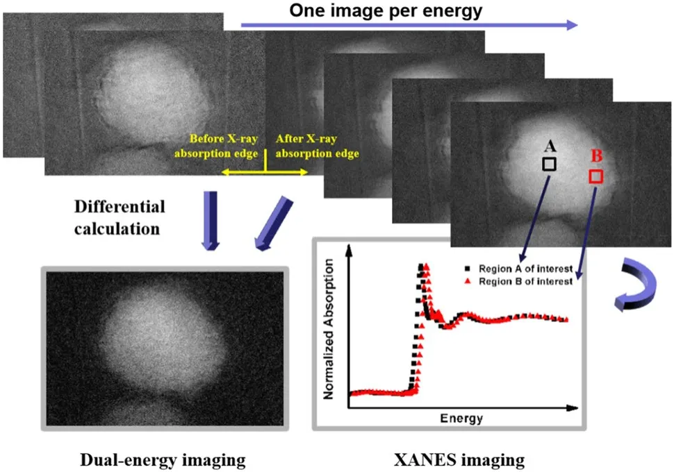
Fig.6 (Color online) The workflow of nano-spectral imaging
Nano-spectral imaging can be classified into dual-energy and TXM-XANES imaging.This concept is illustrated in Fig.6.Dual-energy imaging records projection images at two different energy points: before and after the X-ray absorption edge of the target element.The target element showed a significantly higher absorption edge jump than the other elements in the absorption edge energy region.After the differential calculation of the two images, the enhanced portion of the image displayed the distribution of the target element in the sample.Dual-energy imaging combined with CT technology can be used to obtain the 3D distribution of the target element in a sample.
In a typical XANES experiment, the sample is placed in the middle of two ion chambers, which are used to record the beam intensity during the energy scanning of the monochromator.The absorption coefficients of the target elements were obtained by recording the number of photons in both ion chambers.Accordingly, during XANES imaging, the number of photons that did not pass through the sample was recorded by the imaging detector.When the monochromator performed energy scanning, it recorded a stack of images to calculate the absorption coefficient of the target element.
To extract the absorption spectrum, the stack image underwent a series of steps.The main processing steps for 2D XANES imaging are as follows.
(1) Average projection and reference images.An average number of images can reduce the impact of vibrations on the data and increase the signal-to-noise ratio.
(2) Reference correction to projection images.
(3) Magnification correction and alignment of the lowerenergy projection images.The focal length of the ZP varied linearly with the X-ray energy.During the experiment, the ZP was required to move continuously to maintain its focus at different energies.The projected images at different magnifications were recorded using the detector.Therefore, the image size must match the subtraction of the difference maps.
Once the image processing was completed, an absorption spectrum was generated for each pixel within the region of interest (ROI).After normalizing the spectra, the position of the absorbed edge energy of the target element was determined.The offset of the normalized absorption spectrum was used to characterize the relative valence state changes of the elements.XANES imaging combined with CT technology can be used to obtain 3D valence distribution information of the target element in the sample.The BL18B uses the "TXM-Wizard" software package to perform magnification and misalignment corrections, reference corrections,normalization, and a series of data manipulations on the XANES stack data [24, 25].
3.2 Control and data acquisition system
The control and data acquisition of BL18B were performed using EPICS and a self-designed software [26].EPICS is a suite of open-source software tools, libraries, and applications.It provides a standard distributed control system architecture, communication protocol, runtime database, and software tools and supports a wide range of I/O devices.The in-house-designed software communicates with the EPICS system, realizing motion control of each motor in the experimental station.Instead of using vendor-supplied software, the self-designed software integrates the control of all the important beamline equipment, realizing automatic data collection in TXM, CT, spectral imaging, and other experimental modes.
For TXM and dual-energy imaging, the experimental procedure involved shooting at selected energies.For the CT experiments, the sample was placed at the center of rotation, the experimental energy was selected according to the sample situation; images of the sample projections were captured at different angles.In the XANES experiment,the user can set the energy scanning range and steps in the software interface.As the focal length of the ZP is a function of the incident X-ray energy, the user must capture two clear images at different energies.The software calculates the ZP coordinates corresponding to each energy point based on the ZP positions in the two images, range of scanning energy, and step size required for the experiment.Therefore,during the XANES imaging process, the ZP was moved to keep the sample in focus while the monochromator rotated.Subsequently, the sample was moved in and out to enable the acquisition of the projection with and without the sample under the current energy.For three-dimensional XANES, the program mode collected the CT data at each energy point.
4 VI.Commissioning results
4.1 TXM
A standard Siemens star pattern (Carl Zeiss, German) with the smallest feature size of 30 nm was used for the TXM test in the high-resolution mode.Figure 7a shows an absorption contrast image captured at 8 keV with an exposure time of 30 s.To quantify the spatial resolution of TXM, power spectral density (PSD) analysis was performed on the image data.A 2D Fourier transform was applied to the TXM projection image to calculate the PSD.The 2D power spectral intensity was then integrated over the azimuthal direction(that is, along the circle) at a fixed radial frequency [27–29].Figure 7b shows the PSD result.The cut-offfrequency is 25 μm-1, corresponding to a period of 40 nm, that is, a spatial resolution of 20 nm [30].
We used a piece of dehydrated rabbit bone to test the radiation damage to the biological samples at low energy.Figure 8 shows absorption contrast images of the sample obtained at 5.5 keV, one hour apart.The flux at the sample position was tested using an ionization chamber with a pair of 10-mm long electrodes (IC Plus 10; Oxford, UK).The ionizing current was measured using a high-sensitivity picoammeter (Keithley 6485; Tektronix, USA).The X-ray beam intensities were evaluated using the following equationwhereNis the beam intensity,I0is the measured ionization current,ε0is the gas ionization energy,eis the electron charge,Eis the energy of incident X-ray,xis the electrode length, andμis the absorption coefficientof the filling gas.The number of photons in the sample was approximately 1.26 × 10¹⁰photons/s.Comparing the two images, the sample showed no obvious signs of irradiation damage after one hour of irradiation.
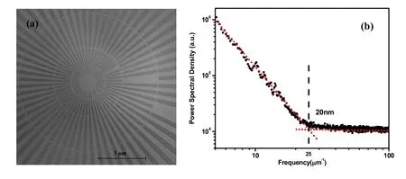
Fig.7 Image of the star pattern:a absorption contrast image and b PSD analysis of (a)
4.2 Nano-CT
Ni-rich LiNi1-x-yCoxMnyO2(NCM) is a commercially available cathodic material.It has several advantages, such as structural stability, low cost, and good cycling performance,etc.[31, 32].Owing to its high nickel content, high performance, and high capacity, LiNi0.6Co0.2Mn0.2O2(NCM622),a typical high-energy cathode, has emerged as an ideal material for automotive applications [33].In the nano-CT experiment, a 50×-cycled NCM622 particle was imaged,and the 3D image was reconstructed.The projections were obtained using an absorption contrast of 8.6 keV.The complete tomography dataset was collected for approximately 6 min with 180 projections (1 s exposure time per projection).The tomography datasets were reconstructed using the AduRecon software.3D reconstruction was performed using the Avizo? Fire software.
It has been reported that in long-cycle, high-rate charging and discharging processes, a series of battery capacity attenuation and battery performance degradation phenomena occur.Correspondingly, during the early stages of the charge and discharge processes, microcracks and radial cracking were observed near the centers of the particles.With an increase in the voltage or cycle time, significant radial cracking inside the particles can be observed [31, 32].A reconstructed 3D image of the NCM622 particle and its slices are shown in Fig.9.The reconstruction results clearly show that the 50×-cycled particle had several cracks inside in an extended state.The CT images had a resolution of 30 nm/pixel.
4.3 2D TXM-XANES
XANES imaging is suitable for investigating battery materials.It correlates mesoscale to nanoscale chemical changes within the secondary particles of the battery electrode, which can reveal the interaction of nano- and micron-scale factors of the macroscopic behavior of battery materials [34].
Pristine and 50×-cycled NCM622 particles were used to test the performance of the 2D TXM-XANES method.Thetarget element is Ni and the experimental energy range is from 8.2 to 8.6 keV.The data were processed to obtain the XANES spectra for each pixel in the ROI.Figure 10 shows the pseudocolor 2D XANES chemical phase maps of Ni within the two particles.The distribution of the absorbed edge energy of the pristine particles is relatively homogeneous, whereas for the cycled particles, the energy of the absorbing edge is lower in the inner region than that in the outer region.The difference in the Ni-ion K-edge absorption energy between the two NCM622 particles is obvious.Figure 10c shows the Ni K-edge XANES spectra of the central portion of Fig.10a, b.The difference between the absorption edges of the two particles is also evident in the spectral line plot.The TXM-XANES imaging method works well for chemical characterization of battery particles in different charging states.

Fig.10 (Color online) Ni element chemical phase maps for NCM622 particles: a pristine particle; b cycled cathode particle; c XANES from two ROIs in (a) and (b)
5 Summary and conclusion
A new in-house designed TXM system was constructed for the SSRF.Herein, we present the characterization of this beamline as well as the commissioning results of TXM,marker-less nano-CT, and TXM-XANES imaging.The beamline will undergo future updates; for instance, the X-ray beam position feedback and correction system will be upgraded for a more stable spot position.Moreover, an angle adjustment motor will be introduced for ZP for better alignment, providing an advanced experimental platform for nanostructure characterization in related disciplines.
Acknowledgements The authors also wish to acknowledge their colleagues from the Department of Beamline Engineering at the SSR for their assistance during the construction of the BL18B beamline.
Author contributions All authors contributed to the study conception and design.Material preparation, data collection, and analysis were performed by Ling Zhang, Fen Tao, Jun Wang, Ruo-Yang Gao,Bo Su, Guo-Hao Du, Ai-Guo Li, Ti-Qiao Xiao, and Biao Deng.The first draft of the manuscript was written by Ling Zhang, and all authors commented on previous versions of the manuscript.All authors read and approved the final manuscript.
Availability of data and materials The data that support the findings of this study are openly available in Science Data Bank at https:// www.doi.org/ 10.57760/ scien cedb.13606 and https:// cstr.cn/ 31253.11.scien cedb.13606.
Declaration
Conflict of interest The authors declare that they have no competing interests.
 Nuclear Science and Techniques2023年12期
- Nuclear Science and Techniques的其它文章
- A machine learning approach to TCAD model calibration for MOSFET
- BL02U1: the relocated macromolecular crystallography beamline at the Shanghai Synchrotron Radiation Facility
- Coin-structured tunable beam shaping assembly design for accelerator-based boron neutron capture therapy for tumors at different depths and sizes
- Simulation study of BESIII with stitched CMOS pixel detector using ACTS
- Advances in nuclear detection and readout techniques
- Enhancing betavoltaic nuclear battery performance with 3D P+PNN+multi-groove structure via carrier evolution